AD724JR View Datasheet(PDF) - Analog Devices
Part Name
Description
Manufacturer
AD724JR Datasheet PDF : 15 Pages
| |||
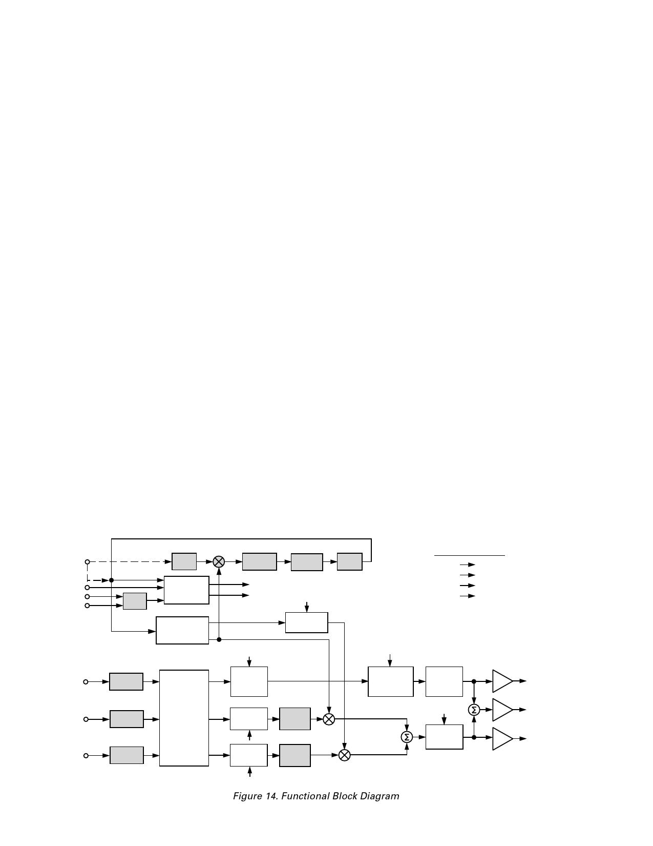
AD724
THEORY OF OPERATION
The AD724 was designed to have three allowable modes of
applying a clock via the FIN pin. These are FSC (frequency of
subcarrier) mode with CMOS clock applied, FSC mode using
on-chip crystal oscillator, and 4FSC mode with CMOS clock
applied. The FSC frequency is 3.579545 MHz for NTSC or
4.433618 MHz for PAL.
To use FSC mode the SELECT pin is pulled low and either a
CMOS FSC clock is applied to FIN, or a parallel-resonant
crystal and appropriate tuning capacitor is placed between the
FIN pin and AGND to utilize the on-chip oscillator. The on-
chip Phase Locked Loop (PLL) is used in these modes to gener-
ate an internal 4FSC clock that is divided to perform the digital
timing as well as create the quadrature subcarrier signals for the
chrominance modulation.
In 4FSC mode, the SELECT pin is pulled high and the PLL is
bypassed.
Referring to the AD724 block diagram (Figure 14), the RGB
inputs (each 714 mV p-p max) are dc clamped using external
coupling capacitors. These clamps allow the user to have a black
level that is not at 0 V. The clamps will adjust to an on-chip
black input signal level of approximately 0.8 V. This clamping
occurs on the back porch during the burst period.
The RGB inputs then pass into an analog encoding matrix,
which creates the luminance (“Y”) signal and the chrominance
color difference (“U” and “V”) signals. The RGB to YUV en-
coding is performed using the following standard transformations:
Y = 0.299 × R + 0.587 × G + 0.114 × B
U = 0.493 × (B–Y)
V = 0.877 × (R–Y)
After the encoding matrix, the AD724 has two parallel analog
paths. The Y (luminance) signal is first passed through a 3-pole
4.85 MHz/6 MHz (NTSC/PAL) Bessel low-pass filter to pre-
vent aliasing in the sampled-data delay line. In this first low-pass
filter, the unclocked sync is injected into the Y signal. The Y
signal then passes through the sampled-data delay line, which is
clocked at 8FSC. The delay line was designed to match the
overall chrominance and luminance delays. Following the
sampled-data delay line is a 5.25 MHz/6.5 MHz (NTSC/PAL)
2-pole low-pass Bessel filter to smooth the reconstructed lumi-
nance signal.
The second analog path is the chrominance path in which the U
and V color difference signals are processed. The U and V sig-
nals first pass through 4-pole modified Bessel low-pass filters
with –3 dB frequencies of 1.2 MHz/1.5 MHz (NTSC/PAL) to
prevent aliasing in the modulators. The color burst levels are
injected into the U channel for NTSC (U and V for PAL) in
these premodulation filters. The U and V signals are then inde-
pendently modulated by a pair of balanced switching modula-
tors driven in quadrature by the color subcarrier.
The bandwidths of the on-chip filters are tuned using propri-
etary auto-tuning circuitry. The basic principle is to match an
RC time constant to a reference time period, that time being
one cycle of a subcarrier clock. The auto-tuning is performed
during the vertical blanking interval and has added hysteresis so
that once an acceptable tuning value is reached the part won’t
toggle tuning values from field to field. The bandwidths stated
in the above discussion are the design target bandwidths for
NTSC and PAL.
The AD724’s 4FSC clock (either produced by the on-chip PLL
or user supplied) drives a digital divide-by-four circuit to create
the quadrature signals for modulation. The reference phase 0° is
used for the U signal. In the NTSC mode, the V signal is modu-
lated at 90°, but in PAL mode, the V modulation alternates
between 90° and 270° at the horizontal line rate as required by
the PAL standard. The outputs of the U and V balanced modu-
lators are summed and passed through a 3-pole low-pass filter with
3.6 MHz/4.4 MHz bandwidths (NTSC/PAL) in order to re-
move the harmonics generated during the switching modulation.
SUB- FSC
CARRIER
4FSC
NTSC/PAL
HSYNC
VSYNC
XOSC
PHASE
DETECTOR
CHARGE
PUMP
4FSC
SYNC
SEPARATOR
XNOR
CSYNC
4FSC
QUADRATURE
+4
DECODER
FSC
CSYNC
BURST
FSC 90؇
FSC 0؇
CSYNC
LOOP
FILTER
4FSC
VCO
NTSC/PAL
±180؇
SC 90؇/270؇
(PAL ONLY)
CLOCK
AT 8FSC
RED
DC
CLAMP
Y
3-POLE
LP PRE-
FILTER
SAMPLED-
DATA
DELAY LINE
GREEN
BLUE
DC
CLAMP
DC
CLAMP
RGB-TO-YUV U
ENCODING
MATRIX
4 -POLE
LPF
V
4 -POLE
LPF
U
CLAMP
V
CLAMP
BALANCED
MODULATORS
BURST
Figure 14. Functional Block Diagram
POWER AND GROUNDS
+5V
LOGIC
+5V
ANALOG
AGND
ANALOG
DGND
LOGIC
NOTE:
THE LUMINANCE, COMPOSITE, AND
CHROMINANCE OUTPUTS ARE AT
TWICE NORMAL LEVELS FOR DRIVING
75⍀ REVERSE-TERMINATED LINES.
2-POLE
LP POST-
FILTER
NTSC/PAL
4-POLE
LPF
X2
LUMINANCE
OUTPUT
X2
COMPOSITE
OUTPUT
CHROMINANCE
X2
OUTPUT
–8–
REV. B
Share Link: 