UPD4726GS-BAF View Datasheet(PDF) - NEC => Renesas Technology
Part Name
Description
Manufacturer
UPD4726GS-BAF Datasheet PDF : 12 Pages
| |||
µPD4726
ELECTRICAL SPECIFICATIONS (RECEIVERS)
(Unless otherwise specified, VCC = 4.5 to 5.5 V, Ta = −40 to +85 °C, C1 through C5 = 1 µF)
Parameter
Symbol
Conditions
Output voltage, low
(STBY = H)
VOL1
IOUT = 4 mA
Output voltage, high
(STBY = H)
VOH1
IOUT = −4 mA
Output voltage, low
(STBY = L)
VOL2
IOUT = 4 mA
Output voltage, high
(STBY = L)
VOH2
IOUT = −4 mA
Propagation delay time
(STBY = H)
Propagation delay time
(STBY = L, EN = H)
Propagation delay time
(STBY = L)
tPHL
RIN → ROUT, CL =150 pF
tPLH
VCC = +4.5 V, Note 11
tPHL
RIN → ROUT (R6, R7), CL =150 pF
tPLH
VCC = +4.5 V, Note 11
tPHA
EN → ROUT (R6, R7), CL =150 pF
tPAH
VCC = +4.5 V, Note 12
Input resistance
RI
Open voltage across input pins VIO
Input threshold voltage
VIH
(STBY = H)
VIL
VCC = +4.5 to +5.5 V
VCC = +4.5 to +5.5 V
VH
VCC = +4.5 to +5.5 V
(hysteresis width)
Input threshold voltage
(STBY = L, EN = H)
VIH
VCC = +4.5 to +5.5 V, RIN6, RIN7
VIL
VCC = +4.5 to +5.5 V, RIN6, RIN7
Standby output transition time
tDAH
Note 13
Standby output transition time
tDHA
Note 13
Power-ON output transition time tPRA Note 14
Remark TYP. value is a reference value at Ta = 25 °C.
MIN. TYP. MAX. Unit
0.4
V
VCC − 0.4
V
0.5
V
VCC − 0.5
V
0.2
µs
0.1
µs
100
300
ns
3
5.5
7
kΩ
0.5
V
1.7
2.3
2.7
V
0.7
1.1
1.7
V
0.5
1.2
1.8
V
2.7
1.5
V
1.5
0.7
V
0.2
3
µs
0.3
1
ms
0.5
1
ms
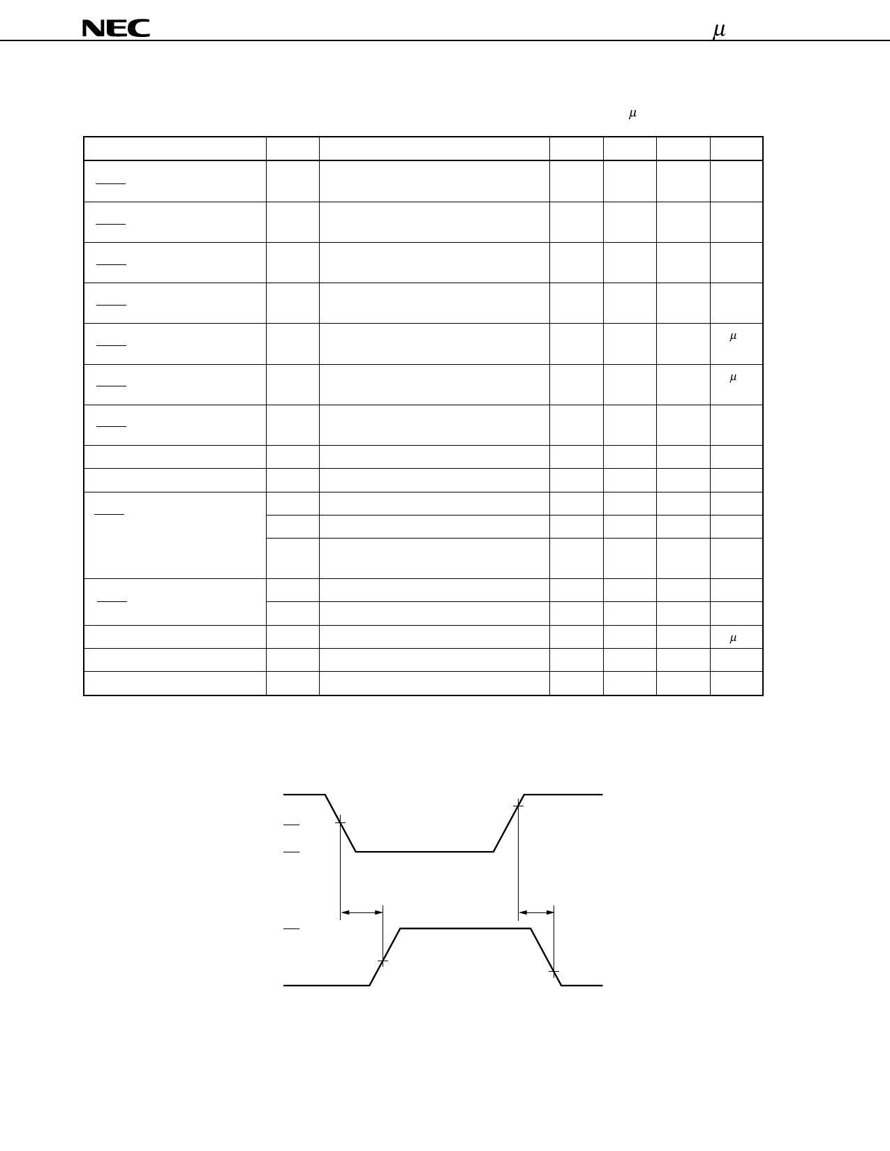
Note 11. Test point
+3 V
RIN 0 V
−3 V
0.7 V
2.7 V
VOH
ROUT
VOL
tPLH
2.0 V
tPHL
0.8 V
8
Share Link: 