MCM32A732SG33 View Datasheet(PDF) - Motorola => Freescale
Part Name
Description
Manufacturer
MCM32A732SG33 Datasheet PDF : 12 Pages
| |||
CAPACITANCE (f = 1 MHz, dV = 3 V, TA = 25°C, Periodically sampled rather than 100% tested)
Characteristic
Cache Address Input Capacitance
Control Pin Input Capacitance
(E, W)
I/O Capacitance
Tag Address Input Capacitance
Symbol
Cin
Cin
CI/O
Cin
Max
Unit
48
pF
8
pF
8
pF
18
pF
AC OPERATING CONDITIONS AND CHARACTERISTICS
(VCC = 5.0 V ± 10%, TA = 0 to + 70°C, Unless Otherwise Noted)
Input Timing Measurement Reference Level . . . . . . . . . . . . . . . 1.5 V
Input Pulse Levels . . . . . . . . . . . . . . . . . . . . . . . . . . . . . . . . . 0 to 3.0 V
Input Rise/Fall Time . . . . . . . . . . . . . . . . . . . . . . . . . . . . . . . . . . . . 5 ns
Output Timing Measurement Reference Level . . . . . . . . . . . . . 1.5 V
Output Load . . . . . . . . . . . . . . . . Figure 1A Unless Otherwise Noted
READ CYCLE (See Notes 1 and 2)
Data
Tag/Valid
Dirty
Parameter
Symbol Min Max Min Max Min Max Unit Notes
Read Cycle Time
Address Access Time
tAVAV 30 — 30 — 30 — ns
3
xCA2–3 tAVQV — 20 — 12 — — ns
9
(Transparent Mode) A4 – A19 tAVQV — 25 — 12 — 25
Chip Select Access Time
tELQV — 20 — 12 — 20 ns
4
Output Enable to Output Valid
tGLQV — 10 — 6 — — ns
Output Hold from Address Change
tAXQX 4 — 4 — 4 — ns 5,6,7
Enable Low to Output Active
tELQX 4 — 4 — 4 — ns 5,6,7
Enable High to Output High–Z
tEHQZ — 9 — 7 — 9 ns 5,6,7
Output Enable Low to Output Active
tGLQX 0 — 0 — 0 — ns 5,6,7
Output Enable High to Output High–Z
tGHQZ — 8 — 6 — — ns 5,6,7
NOTES:
1. W is high for read cycle.
2. E = Exx, ET; W = Wxx, WT, WA; G = GA, GB
3. All timings are referenced from the last valid address to the first transitioning address.
4. Addresses valid prior to or coincident with E going low.
5. At any given voltage and temperature, tEHQZ (max) is less than tELQX (min), and tGHQZ (max) is less than tGLQX (min), both for a given
device and from device to device.
6. Transition is measured ±500 mV from steady–state voltage with load of Figure 1B.
7. This parameter is sampled and not 100% tested.
8. Device is continuously selected (E = VIL, G = VIL).
9. TAG Address Access Time tAVTV.
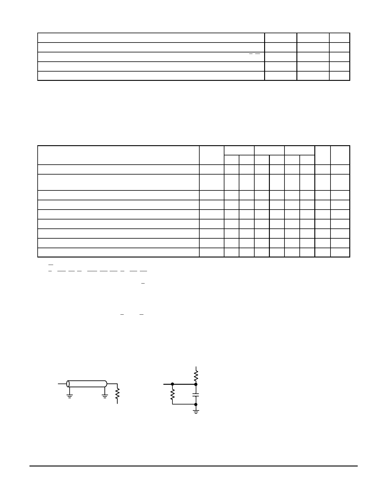
OUTPUT
AC TEST LOADS
Z0 = 50 Ω
50 Ω
VL = 1.5 V
OUTPUT
255 Ω
+5 V
480 Ω
5 pF
Figure 1A
Figure 1B
TIMING LIMITS
The table of timing values shows either a
minimum or a maximum limit for each param-
eter. Input requirements are specified from
the external system point of view. Thus, ad-
dress setup time is shown as a minimum
since the system must supply at least that
much time (even though most devices do not
require it). On the other hand, responses from
the memory are specified from the device
point of view. Thus, the access time is shown
as a maximum since the device never pro-
vides data later than that time.
MCM32A732/764•MCM32A832/864•MCM32A932/964
6
MOTOROLA FAST SRAM
Share Link: 