ICS9110-01CS14 View Datasheet(PDF) - Integrated Circuit Systems
Part Name
Description
Manufacturer
ICS9110-01CS14 Datasheet PDF : 10 Pages
| |||
AV9110
Absolute Maximum Ratings
Supply Voltage . . . . . . . . . . . . . . . . . . . . . . . . . . 7.0 V
Voltage on I/O pins referenced to GND . . . . . . GND –0.5 V to VDD +0.5 V
Operating Temperature under bias . . . . . . . . . . 0°C to +70°C
Power dissipation . . . . . . . . . . . . . . . . . . . . . . . . 0.8 Watts
Storage Temperature . . . . . . . . . . . . . . . . . . . . . . –65°C to +150°C
Stresses above those listed under Absolute Maximum Ratings may cause permanent damage to the device. These ratings are
stress specifications only and functional operation of the device at these or any other conditions above those listed in the
operational sections of the specifications is not implied. Exposure to absolute maximum rating conditions for extended
periods may affect product reliability.
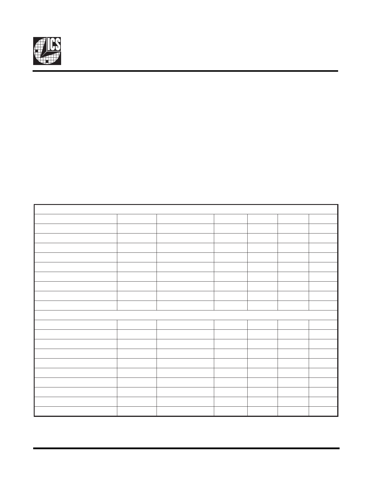
Electrical Characteristics
VDD = +5V±10%, TA = 0 – 70° C unless otherwise stated
PARAMETER
Input Low Voltage
Input High Voltage
Input Low Current
Input High Current
Output Low Voltage1
Output High Voltage1
Input Clock Rise Time1
Input Clock Fall Time1
Supply Current
Output frequency range
Rise time, 20-80%1
Fall time, 80-20%1
Duty cycle1 @ 50%
Jitter, 1 sigma1
Jitter, absolute1
Input reference freq.; AV9110-011
Input reference freq.; AV9110-021
Input DATA or SCLK frequency1
Skew, Output to Output/X1
DC/STATIC
SYMBOL TEST CONDITIONS
VIL
VIH
IIL
IIH
VOL
V I = 8Ma
OH OH
ICLKr
ICLKf
IDD
VDD = 5V
VDD = 5V
VIN = OV
VIN = VDD
IOL = 8Ma
No load
AC/DYNAMIC
fo
tr
25pF load
tf
25pF load
dt
25pF load
fREF
fREF
f
DATA
tskew
Crystal input
TTL input
MIN
-
2.0
-
-
-
2.4
-
-
-
0.78
-
-
40
-
-
5
0.6
-
-
TYP
-
-
-
-
-
-
-
-
25
-
-
-
-
±40
±125
14.318
14.318
-
400
MAX
0.8
-
-5
5
0.4
-
20
20
-
130
3
3
60
-
-
32
32
32
-
UNITS
V
V
µA
µA
V
V
ns
ns
mA
MHz
ns
ns
%
ps
ps
MHz
MHz
MHz
ps
Note 1: Parameter is guaranteed by design and characterization. Not 100% tested in production.
3
Share Link: 