NT5SV16M8CT View Datasheet(PDF) - Nanya Technology
Part Name
Description
Manufacturer
NT5SV16M8CT Datasheet PDF : 66 Pages
| |||
NT5SV32M4CT
NT5SV16M8CT
NT5SV8M16CT
128Mb Synchronous DRAM
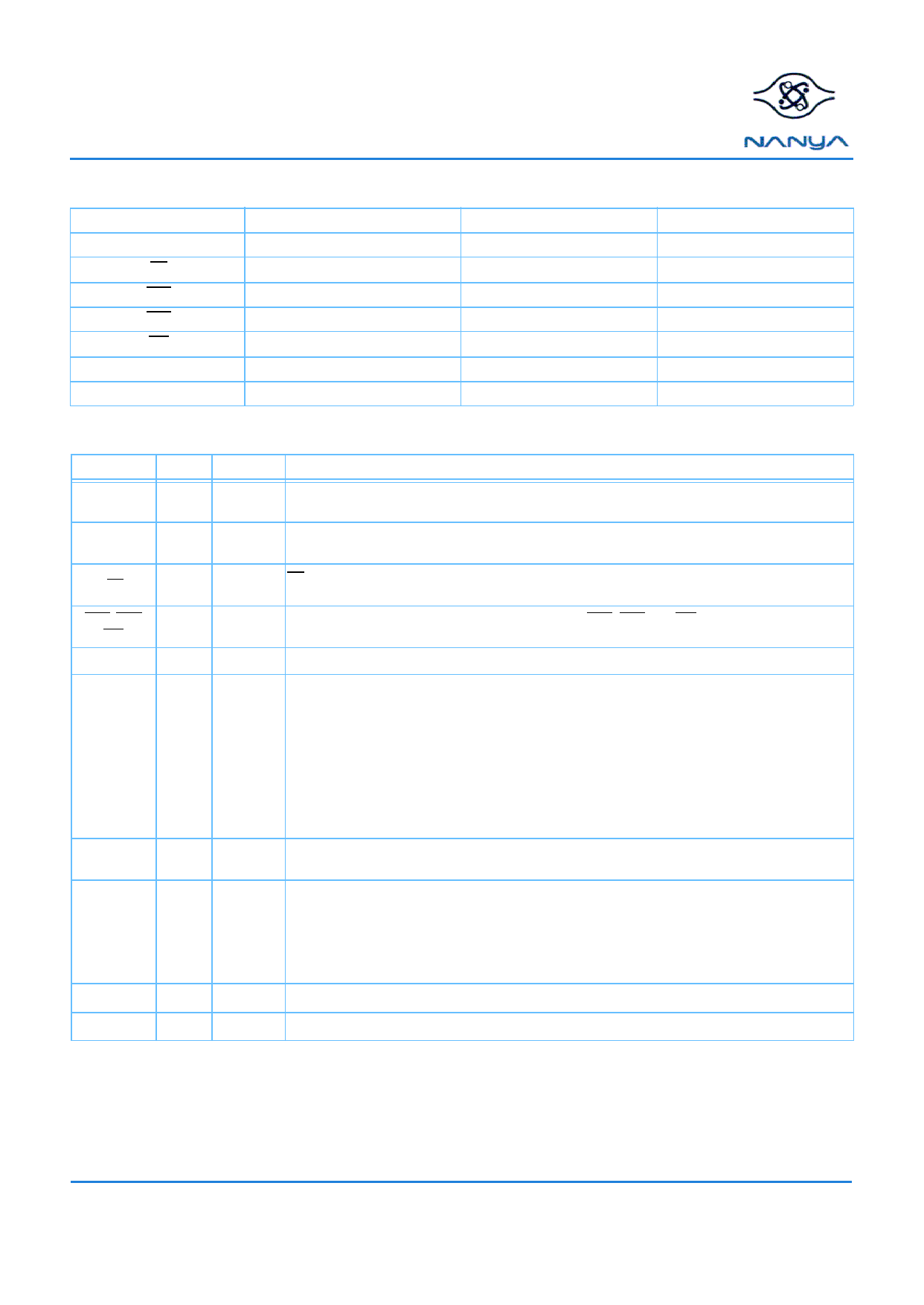
Pin Description
CK
CKE
CS
RAS
CAS
WE
BS1, BS0
A0 - A11
Clock Input
Clock Enable
Chip Select
Row Address Strobe
Column Address Strobe
Write Enable
Bank Select
Address Inputs
DQ0-DQ15
DQM, LDQM, UDQM
VDD
VSS
VDDQ
V SSQ
NC
—
Data Input/Output
Data Mask
Power (+3.3V)
Ground
Power for DQs (+3.3V)
Ground for DQs
No Connection
—
Input/Output Functional Description
Symbol
Type
Polarity
Function
CLK
Input
Positive
Edge The system clock input. All of the SDRAM inputs are sampled on the rising edge of the clock.
CKE
Input Active High Activates the CLK signal when high and deactivates the CLK signal when low. By deactivating the
clock, CKE low initiates the Power Down mode, Suspend mode, or the Self Refresh mode.
CS
Input Active Low CS enables the command decoder when low and disables the command decoder when high. When the
command decoder is disabled, new commands are ignored but previous operations continue.
RAS, CAS,
WE
When sampled at the positive rising edge of the clock, CAS , RAS , and WE define the operation to be
Input Active Low
executed by the SDRAM.
BS0, BS1
Input
—
Selects which bank is to be active.
A0 - A11
Input
During a Bank Activate command cycle, A0-A11 defines the row address (RA0-RA11) when sampled at
the rising clock edge.
During a Read or Write command cycle, A0-A9 and A11 defines the column address (CA0-CA9, CA11)
when sampled at the rising clock edge.
—
A10 is used to invoke auto-precharge operation at the end of the burst read or write cycle. If A10 is
high, auto-precharge is selected and BS0, BS1 defines the bank to be precharged. If A10 is low, auto-
precharge is disabled.
During a Precharge command cycle, A10 is used in conjunction with BS0, BS1 to control which bank(s)
to precharge. If A10 is high, all banks will be precharged regardless of the state of BS. If A10 is low,
then BS0 and BS1 are used to define which bank to precharge.
DQ0 - DQ15 Input-
—
Data Input/Output pins operate in the same manner as on conventional DRAMs.
Output
DQM
LDQM
UDQM
Input
The Data Input/Output mask places the DQ buffers in a high impedance state when sampled high. In
x16 products, LDQM and UDQM control the lower and upper byte I/O buffers, respectively. In Read
Active High mode, DQM has a latency of two clock cycles and controls the output buffers like an output enable.
DQM low turns the output buffers on and DQM high turns them off. In Write mode, DQM has a latency
of zero and operates as a word mask by allowing input data to be written if it is low but blocks the write
operation if DQM is high.
VD D, VSS
Supply
—
Power and ground for the input buffers and the core logic.
V DDQ VSSQ Supply
—
Isolated power supply and ground for the output buffers to provide improved noise immunity.
REV 1.0
May, 2001
3
© NANYA TECHNOLOGY CORP. All rights reserved.
NANYA TECHNOLOGY CORP. reserves the right to change Products and Specifications without notice.
Share Link: 