NT5SV16M8CT View Datasheet(PDF) - Nanya Technology
Part Name
Description
Manufacturer
NT5SV16M8CT Datasheet PDF : 66 Pages
| |||
NT5SV32M4CT
NT5SV16M8CT
NT5SV8M16CT
128Mb Synchronous DRAM
Bank Activate Command
In relation to the operation of a fast page mode DRAM, the Bank Activate command correlates to a falling RAS signal. The Bank
Activate command is issued by holding CAS and WE high with CS and RAS low at the rising edge of the clock. The Bank Select
address BS0 - BS1 is used to select the desired bank. The row address A0 - A11 is used to determine which row to activate in
the selected bank.
The Bank Activate command must be applied before any Read or Write operation can be executed. The delay from when the
Bank Activate command is applied to when the first read or write operation can begin must meet or exceed the RAS to CAS
delay time (tRCD). Once a bank has been activated it must be precharged before another Bank Activate command can be
applied to the same bank. The minimum time interval between successive Bank Activate commands to the same bank is deter-
mined by the RAS cycle time of the device (tRC). The minimum time interval between interleaved Bank Activate commands
(Bank A to Bank B and vice versa) is the Bank to Bank delay time (tRRD). The maximum time that each bank can be held active
is specified as tRAS(max).
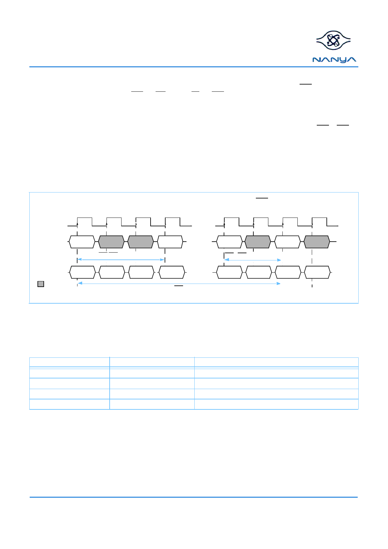
Bank Activate Command Cycle
T0
T1
T2
CK
ADDRESS
Bank A
Row Addr.
R A S-CAS delay (tRCD)
COMMAND
: “H” or “L”
Bank A
Activate
NOP
NOP
(CAS Latency = 3, tRCD = 3)
T3
Tn
Tn+1
Tn+2
Tn+3
..........
Bank A
Col. Addr.
..........
Bank B
Row Addr.
Bank A
Row Addr.
R A S - R A S delay time (tRRD)
Write A
with Auto
Precharge
..........
Bank B
Activate
NOP
Bank A
Activate
RAS Cycle time ( tRC )
NOP
Bank Select
The Bank Select inputs, BS0 and BS1, determine the bank to be used during a Bank Activate, Precharge, Read, or Write oper-
ation.
Bank Selection Bits
BS0
BS1
0
0
1
0
0
1
1
1
Bank
Bank 0
Bank 1
Bank 2
Bank 3
REV 1.0
May, 2001
9
© NANYA TECHNOLOGY CORP. All rights reserved.
NANYA TECHNOLOGY CORP. reserves the right to change Products and Specifications without notice.
Share Link: 