V54C3128164VALS6 View Datasheet(PDF) - Mosel Vitelic Corporation
Part Name
Description
Manufacturer
V54C3128164VALS6
Mosel Vitelic Corporation

V54C3128164VALS6 Datasheet PDF : 49 Pages
| |||
MOSEL VITELIC
V54C3128(16/80/40)4V(T/S)
128Mbit SDRAM
3.3 VOLT, TSOP II / SOC PACKAGE
8M X 16, 16M X 8, 32M X 4
PRELIMINARY
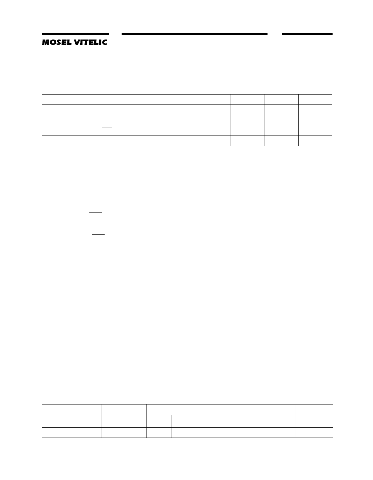
System Frequency (fCK)
Clock Cycle Time (tCK3)
Clock Access Time (tAC3) CAS Latency = 3
Clock Access Time (tAC2) CAS Latency = 2
6
166 MHz
6 ns
5.4 ns
5.4 ns
7PC
143 MHz
7 ns
5.4 ns
5.4 ns
7
143 MHz
7 ns
5.4 ns
6 ns
8PC
125 MHz
8 ns
6 ns
6 ns
Features
■ 4 banks x 2Mbit x 16 organization
■ 4 banks x 4Mbit x 8 organization
■ 4 banks x 8Mbit x 4 organization
■ High speed data transfer rates up to 166 MHz
■ Full Synchronous Dynamic RAM, with all signals
referenced to clock rising edge
■ Single Pulsed RAS Interface
■ Data Mask for Read/Write Control
■ Four Banks controlled by BA0 & BA1
■ Programmable CAS Latency: 2, 3
■ Programmable Wrap Sequence: Sequential or
Interleave
■ Programmable Burst Length:
1, 2, 4, 8 for Sequential Type
1, 2, 4, 8 for Interleave Type
■ Multiple Burst Read with Single Write Operation
■ Automatic and Controlled Precharge Command
■ Random Column Address every CLK (1-N Rule)
■ Power Down Mode
■ Auto Refresh and Self Refresh
■ Refresh Interval: 4096 cycles/64 ms
■ Available in 60-ball SOC BGA and 54 Pin
TSOPII
■ LVTTL Interface
■ Single +3.3 V ±0.3 V Power Supply
Description
The V54C3128(16/80/40)4V(T/S) is a four bank
Synchronous DRAM organized as 4 banks x 2Mbit
x 16, 4 banks x 4Mbit x 8, or 4 banks x 8Mbit x 4.
The V54C3128(16/80/40)4V(T/S) achieves high
speed data transfer rates up to 166 MHz by employ-
ing a chip architecture that prefetches multiple bits
and then synchronizes the output data to a system
clock
All of the control, address, data input and output
circuits are synchronized with the positive edge of
an externally supplied clock.
Operating the four memory banks in an inter-
leaved fashion allows random access operation to
occur at higher rate than is possible with standard
DRAMs. A sequential and gapless data rate of up to
166 MHz is possible depending on burst length,
CAS latency and speed grade of the device.
Device Usage Chart
Operating
Temperature
Range
0°C to 70°C
Package Outline
T/S
6
•
•
Access Time (ns)
7PC
7
•
•
8PC
•
Power
Std.
L
•
•
Temperature
Mark
Blank
V54C3128(16/80/40)4V(T/S) Rev. 1.5 March 2003
1
Share Link: