VN920SO(2013) View Datasheet(PDF) - STMicroelectronics
Part Name
Description
Manufacturer
VN920SO Datasheet PDF : 35 Pages
| |||
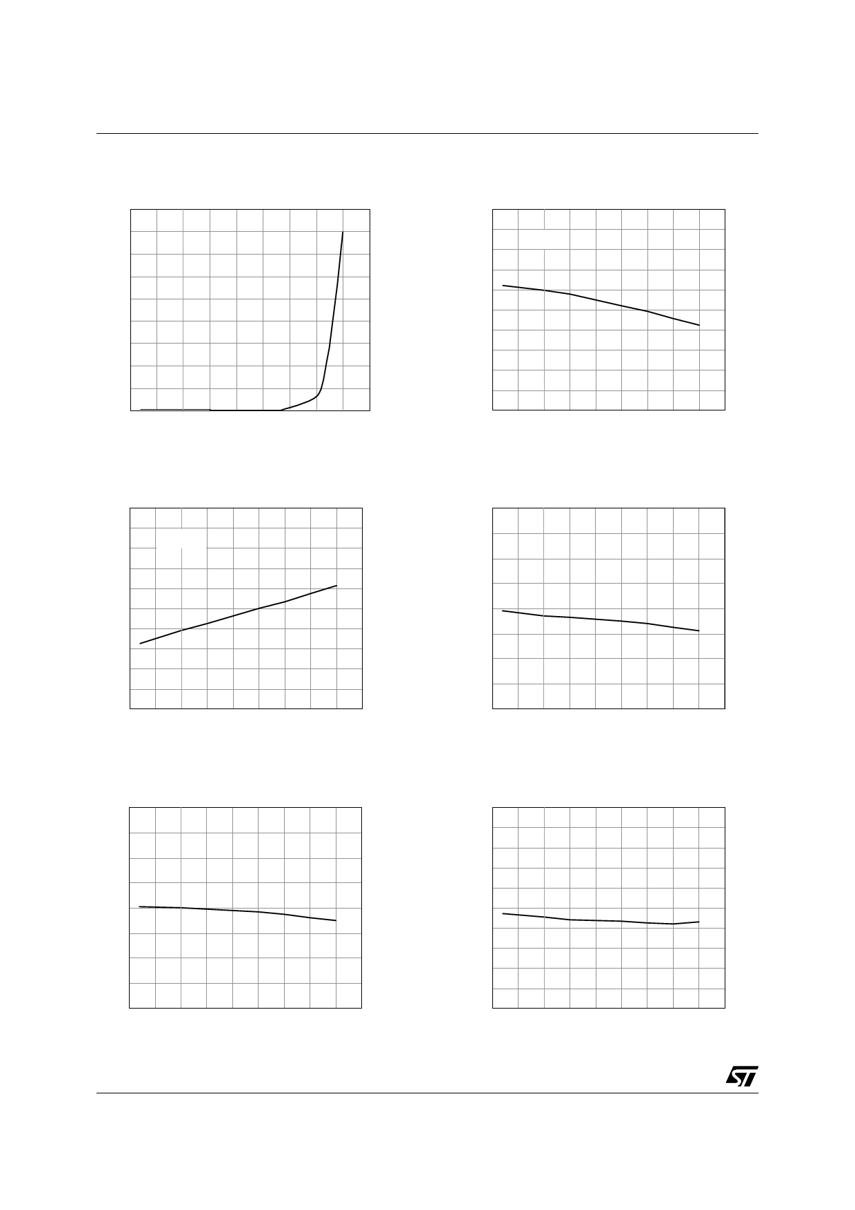
Electrical specifications
VN920
Table 8. Current sense (9V ≤VCC ≤16V) (continued)
Symbol
Parameter
Test conditions
RVSENSEH
Analog sense
output
impedance in
over-temperature
condition
VCC = 13V; Tj > TTSD;
output open
tDSENSE
Current sense
delay response
To 90% ISENSE(1)
1. Current sense signal delay after positive input slope.
Min. Typ. Max. Unit
400
Ω
500 µs
Table 9.
Symbol
VF
VCC output diode
Parameter
Forward on voltage
Test conditions
- IOUT = 5A; Tj = 150°C
Min. Typ. Max. Unit
0.6 V
Table 10. Protections(1)
Symbol
Parameter
Test conditions
Min. Typ. Max. Unit
TTSD
TR
Thyst
Ilim
Shutdown temperature
Reset temperature
Thermal hysteresis
Current limitation
Turn-off output clamp
Vdemag voltage
VCC = 13V
5V < VCC < 36V
IOUT = 2 A;
VIN = 0V;
L = 6mH
150
175
200 °C
135
°C
7
15
°C
30
45
75
A
75
A
VCC - 41 VCC - 48 VCC - 55 V
VON
Output voltage drop
limitation
IOUT = 1 A;
Tj = -40°C...150°C
50
mV
1. To ensure long term reliability under heavy over-load or short circuit conditions, protection and related
diagnostic signals must be used together with a proper software strategy. If the device operates under
abnormal conditions this software must limit the duration and number of activation cycles.
10/34
Share Link: 