VN920-B5 View Datasheet(PDF) - STMicroelectronics
Part Name
Description
Manufacturer
VN920-B5 Datasheet PDF : 25 Pages
| |||
VN920 / VN920-B5 / VN920SO
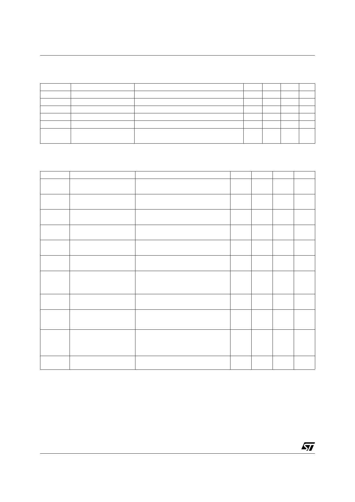
ELECTRICAL CHARACTERISTICS (continued)
LOGIC INPUT
Symbol
VIL
IIL
VIH
IIH
VI(hyst)
VICL
Parameter
Input Low Level
Low Level Input Current
Input High Level
High Level Input Current
Input Hysteresis Voltage
Input Clamp Voltage
VIN=1.25V
VIN=3.25V
IIN=1mA
IIN=-1mA
Test Conditions
Note 1: Vclamp and VOV are correlated. Typical difference is 5V.
CURRENT SENSE (9V≤VCC≤16V) (See Fig. 1)
Symbol
Parameter
Test Conditions
K1
dK1/K1
K2
dK2/K2
K3
dK3/K3
IOUT/ISENSE
Current Sense Ratio Drift
IOUT/ISENSE
Current Sense Ratio Drift
IOUT/ISENSE
Current Sense Ratio Drift
IOUT=1A; VSENSE=0.5V;
Tj= -40°C...150°C
IOUT=1A; VSENSE=0.5V;
Tj= -40°C...+150°C
IOUT=10A; VSENSE=4V; Tj=-40°C
Tj=25°C...150°C
IOUT=10A; VSENSE=4V;
Tj=-40°C...+150°C
IOUT=30A; VSENSE=4V; Tj=-40°C
Tj=25°C...150°C
IOUT=30A; VSENSE=4V;
Tj=-40°C...+150°C
ISENSEO
Analog Sense Leakage
Current
VCC=6...16V; IOUT=0A;VSENSE=0V;
Tj=-40°C...+150°C
VSENSE
VSENSEH
RVSENSEH
tDSENSE
Max Analog Sense Output
Voltage
Sense Voltage in
Overtemperature
conditions
VCC=5.5V; IOUT=5A; RSENSE=10KΩ
VCC>8V; IOUT=10A; RSENSE=10KΩ
VCC=13V; RSENSE=3.9KΩ
Analog Sense Output
Impedance in
Overtemperature
Condition
VCC=13V; Tj>TTSD; Output Open
Current sense delay
response
to 90% ISENSE (see note 2)
Note 2: current sense signal delay after positive input slope.
Min Typ Max Unit
1.25 V
1
µA
3.25
V
10 µA
0.5
V
6
6.8
8
V
-0.7
V
Min Typ Max Unit
3300 4400 6000
-10
+10
%
4200
4400
4900
4900
6000
5750
-8
+8
%
4200
4400
4900
4900
5500
5250
-6
+6
%
0
10
µA
2
V
4
V
5.5
V
400
Ω
500
µs
4/25
Share Link: 