VES9600 View Datasheet(PDF) - Philips Electronics
Part Name
Description
Manufacturer
VES9600 Datasheet PDF : 16 Pages
| |||
Philips Semiconductors
Single Chip DVB-T Channel Receiver
Product specification
VES9600
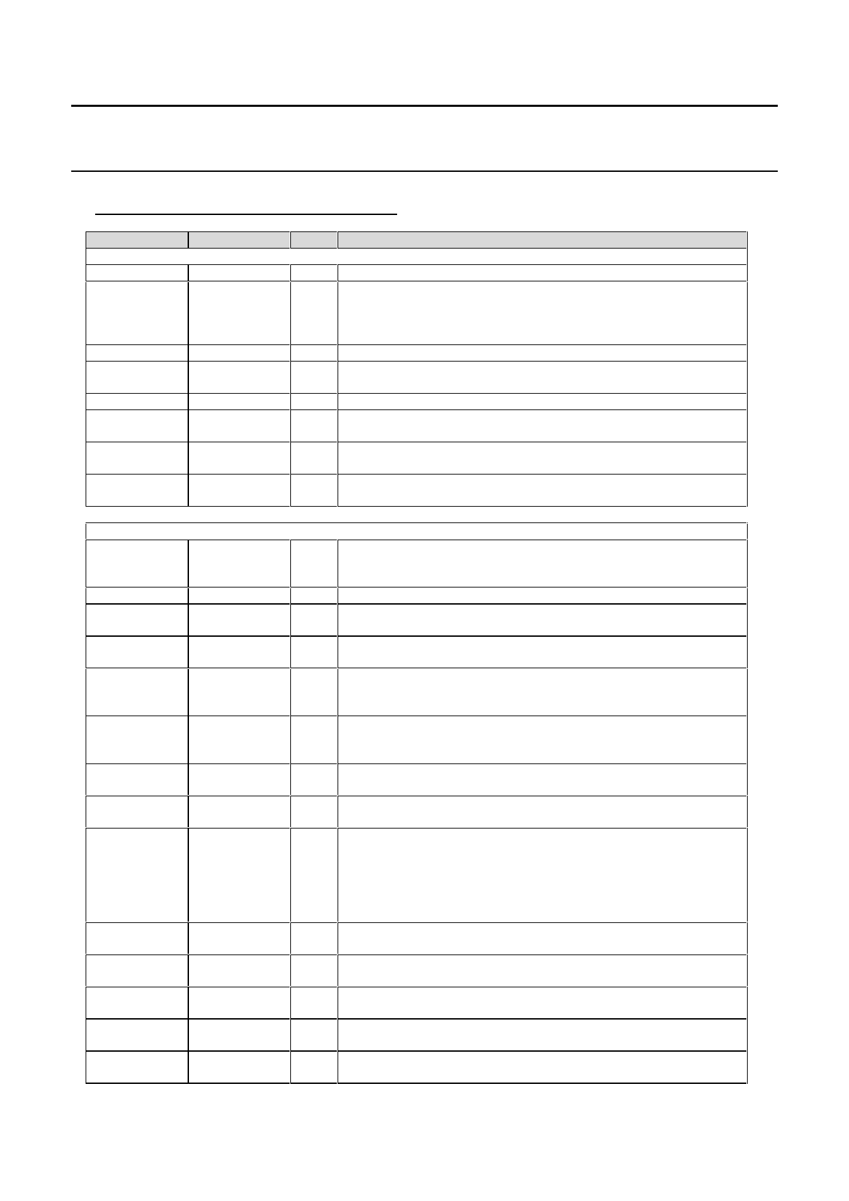
INPUT - OUTPUT SIGNAL DESCRIPTION
SYMBOL
CLR#
XIN
XOUT
SACLK
USE_NCO
CTRL_VCXO
CLK_X1
CLK_X2
PIN NUMBER
32
8
9
25
33
26
181
180
TYPE
DESCRIPTION
CLOCK AND RESET SIGNALS
I
reset signal, active low
Crystal oscillator input pin. When USE_NCO pin is high a third
I
overtone XTAL should be connected between the XIN and XOUT pins.
When USE_NCO pin is low a VCXO should be connected between
XIN and via a RC filter to the CTRL_VCXO output.
O
Crystal oscillator output pin.
O
Sampling frequency output. This output clock can be fed to an
(5V)
external (10-bit) ADC as sampling clock. SACLK= XIN/2
I
When low the chip is in VCXO mode else in NCO mode
O If not in NCO mode, control of an external sampling VCXO (after low-
(5V)
pass filtering)
O
(5V)
Internal SACLK equivalent monitoring output.
O
(5V)
Internal SACLK* 2 equivalent monitoring output.
FI[9:0]
12-13-14-15-16-
19-20-21-22-23
FFT_WIN_IN
81
FFT_WIN_OUT
82
VAGC
27
RECOV_DATA 168-169-170-
[7:0]
171-172-173-
174-175
CFND[3 :0] 151-152-153-154
H2[3:0] 160-161-162-163
EN_CLK
150
D_START
145
D_VAL
144
FRAME
147
SUPER_FRAME
146
TPS_VAL
143
FEL
77
DEMODULATOR SIGNALS
I Input data from an external ADC, FI must be tied to ground when not
used, positive notation (from 0 to 1023) or two’s complement notation
(from -512 to 511).
I
to be connected to FFT_WIN_OUT in default mode.
O Output signal, indicating the start of the active data; equals 1 during
(3.3)
complex sample 0 of the active FFT block
O output value from the Delta-Sigma Modulator, used to control a log-
(5V)
scaled amplifier (after analog filtering )
O Demodulator output signal (after channel correction), synchronous with
(3.3) the falling edge of CLK_X1, provided in a multiplexed way, I first.
Normal order.
O Multiplexed output bearing the confidence factor during I and channel
(3.3) response square amplitude during Q (4 MSB bits), respectively to
RECOV_DATA. (For the channel square amplitude see C2_H2)
O 4 LSB bits of the channel response square amplitude according to
(3.3)
CFND.
O
enable clk18 to synchronize and phase the RECOV_DATA H2 et
(3.3)
CFND outputs. EN_CLK is set to 1 during I and 0 during Q.
O
Output signal, indicating the start of the active data out of the
(3.3) equalizer; equals 1 during sample Kmin of the RECOV_DATA current
output block, for 2 18MHz clock cycles. CAUTION : sample Kmin does
not convey regular data, since it happens to be a continual carrier; it is
the first active (non zero) sample of the current OFDM block, but
D_VAL and TPS_VAL (see below) will be low.
O
(3.3)
active when RECOV_DATA corresponds to regular data .
O
Indicate the active data out of the first block in a frame at the
(3.3)
demodulation part output. (RECOV_DATA)
O Same as FRAME in 8K; in 2K, active only on the first block of each
(3.3) superframe. Indicates the beginning of a new SUPER-FRAME.
O
(3.3)
active when RECOV_DATA corresponds to TPS demodulated data .
0 front end lock. FEL is an output drain output and therefore requires an
(5V)
external pull up resistor.
1999 Sep 01
4
Share Link: 