LTC1545CG View Datasheet(PDF) - Linear Technology
Part Name
Description
Manufacturer
LTC1545CG Datasheet PDF : 16 Pages
| |||
LTC1545
APPLICATIONS INFORMATION
GENERATOR
BALANCED
INTERCONNECTING
CABLE
LOAD
CABLE
TERMINATION
RECEIVER
A
A'
C
C'
1545 F16
Figure 16. Typical V.28 Interface
A'
A
R1 LTC1344A
51.5Ω
R5
R8 20k
6k
S1
S3
R3
S2 124Ω
R2
51.5Ω
B'
C'
R4
B
20k
GND
LTC1543
LTC1545
R6
10k
RECEIVER
R7
10k
1545 F17
Figure 17. V.28 Receiver Configuration
GENERATOR
BALANCED
INTERCONNECTING
CABLE
LOAD
CABLE
TERMINATION
RECEIVER
A
A'
50Ω
125Ω
50Ω
125Ω
50Ω
B
50Ω
B'
C
C'
1545 F18
Figure 18. Typical V.35 Interface
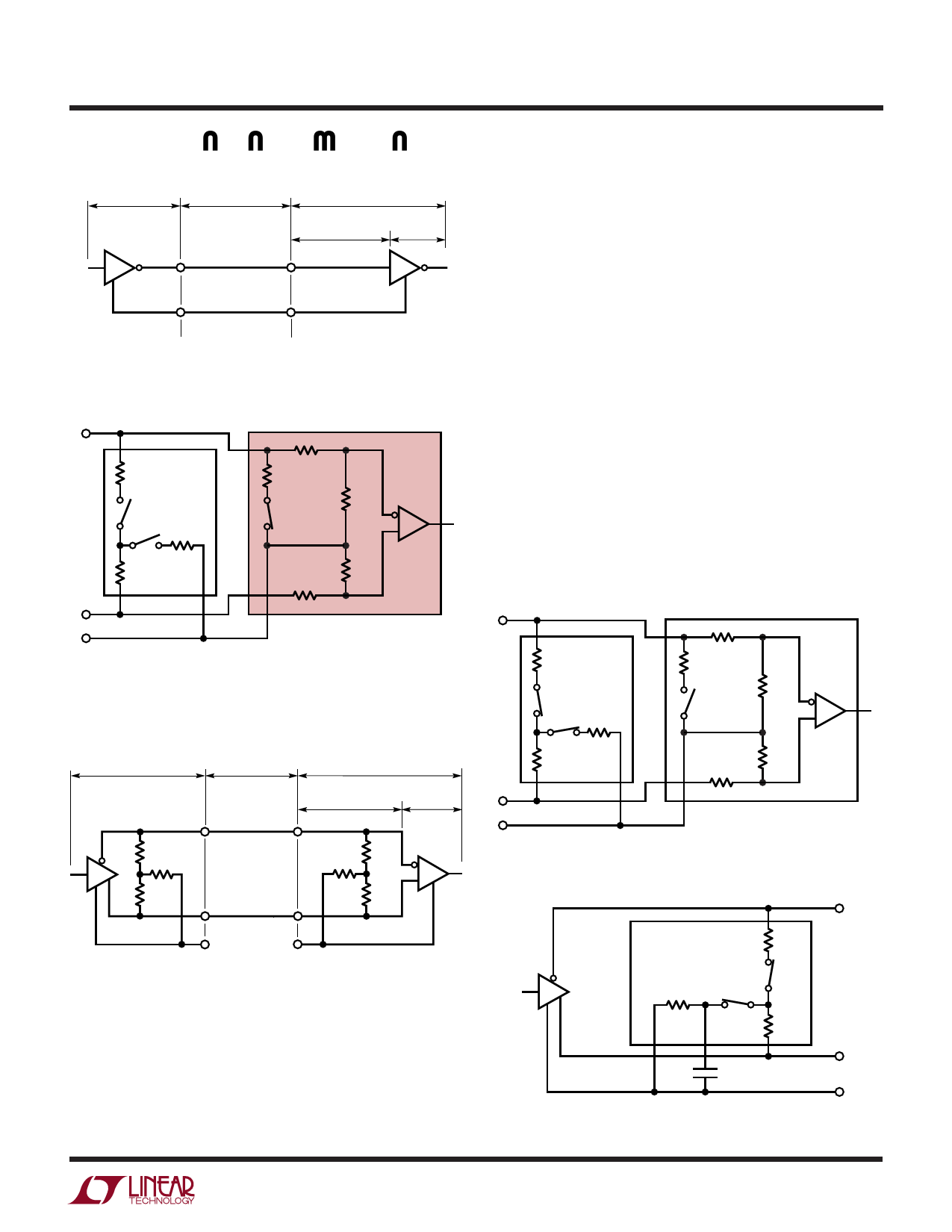
V.35 Interface
A typical V.35 balanced interface is shown in Figure 18. A
V.35 differential generator with outputs A and B with
ground C is connected to a differential receiver with
ground C', inputs A' connected to A, B' connected to B. The
V.35 interface requires a T or delta network termination at
the receiver end and the generator end. The receiver
differential impedance measured at the connector must be
100Ω␣ ±10Ω, and the impedance between shorted termi-
nals (A' and B') and ground C' must be 150Ω ±15Ω.
In V.35 mode, both switches S1 and S2 inside the LTC1344A
are on, connecting the T network impedance as shown in
Figure 19. Both switches in the LTC1543 are off. The 30k
input impedance of the receiver is placed in parallel with
the T network termination, but does not affect the overall
input impedance significantly.
The generator differential impedance must be 50Ω to
150Ω and the impedance between shorted terminals (A
and B) and ground C must be 150Ω ±15Ω. For the
generator termination, switches S1 and S2 are both on and
the top side of the center resistor is brought out to a pin so
it can be bypassed with an external capacitor to reduce
common mode noise as shown in Figure 20.
A'
A
R1 LTC1344A
51.5Ω
R5
R8 20k
6k
S1
R3
S3
S2 124Ω
R2
51.5Ω
B'
C'
R4
B
20k
GND
LTC1543
R6 RECEIVER
10k
R7
10k
1545 F19
Figure 19. V.35 Receiver Configuration
A
LTC1344A
V.35 DRIVER
124Ω
51.5Ω
S1
S2
ON
ON
C1
100pF
51.5Ω
B
C
1545 F20
Figure 20. V.35 Driver Using the LTC1344A
11
Share Link: 