LTC1545CG View Datasheet(PDF) - Linear Technology
Part Name
Description
Manufacturer
LTC1545CG Datasheet PDF : 16 Pages
| |||
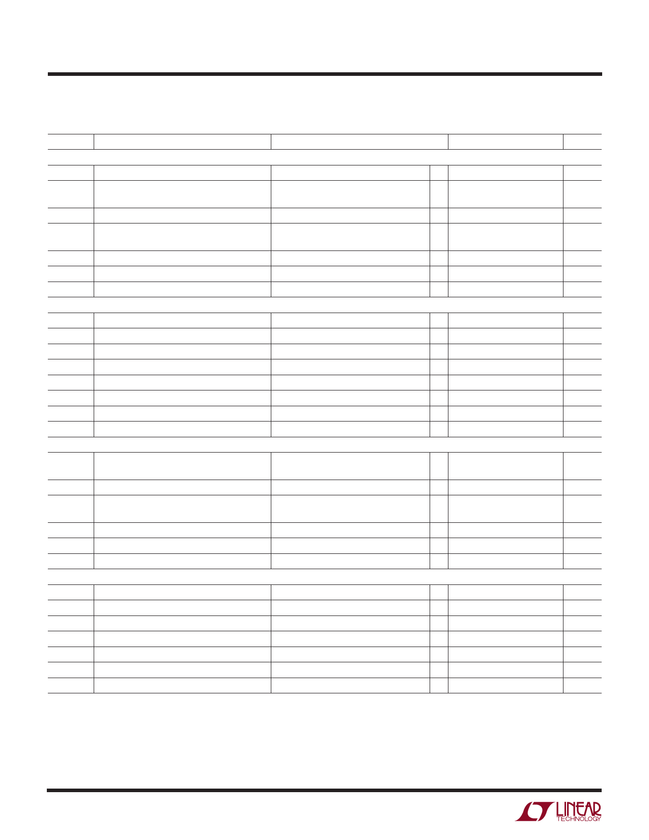
LTC1545
ELECTRICAL CHARACTERISTICS
The q denotes specifications which apply over the full operating temperature range, otherwise specifications are at TA = 25°C.
VCC = 5V, VDD = 8V, VEE = – 7V for V.28, – 5.5V for V.10, V.11 (Notes 2, 3)
SYMBOL PARAMETER
CONDITIONS
MIN TYP MAX
V.10 Driver
VO
Output Voltage
VT
Output Voltage
ISS
Short-Circuit Current
IOZ
Output Leakage Current
Open Circuit, RL = 3.9k
RL = 450Ω (Figure 3)
RL = 450Ω (Figure 3)
VO = GND
– 0.25V ≤ VO ≤ 0.25V, Power Off or
No-Cable Mode or Driver Disabled
q ±4
±6
q ±3.6
0.9VO
±150
q
±0.1 ±100
tr, tf
Rise or Fall Time
t PLH
Input to Output
t PHL
Input to Output
V.10 Receiver
RL = 450Ω, CL = 100pF (Figures 3, 7)
2
RL = 450Ω, CL = 100pF (Figures 3, 7)
1
RL = 450Ω, CL = 100pF (Figures 3, 7)
1
VTH
∆VTH
IIN
RIN
tr, tf
tPLH
tPHL
∆t
V.28 Driver
Receiver Input Threshold Voltage
Receiver Input Hysteresis
Receiver Input Current
Receiver Input Impedance
Rise or Fall Time
Input to Output
Input to Output
Input to Output Difference, tPLH – tPHL
– 10V ≤ VA ≤ 10V
– 10V ≤ VA ≤ 10V
(Figures 4, 8)
(Figures 4, 8)
(Figures 4, 8)
(Figures 4, 8)
q – 0.25
0.25
q
25
50
q
± 0.66
q 15
30
15
55
109
60
VO
Output Voltage
ISS
Short-Circuit Current
IOZ
Output Leakage Current
Open Circuit
RL = 3k (Figure 3)
VO = GND
– 0.25V ≤ VO ≤ 0.25V, Power Off or
No-Cable Mode or Driver Disabled
q
q ±5
q
q
± 10
±8.5
±150
±1 ±100
SR
Slew Rate
t PLH
Input to Output
t PHL
Input to Output
V.28 Receiver
RL = 3k, CL = 2500pF (Figures 3, 7)
RL = 3k, CL = 2500pF (Figures 3, 7)
RL = 3k, CL = 2500pF (Figures 3, 7)
q
4
q
q
30
1.3
2.5
1.3
2.5
VTHL
VTLH
∆VTH
RIN
tr, tf
tPLH
tPHL
Input Low Threshold Voltage
Input High Threshold Voltage
Receiver Input Hysterisis
Receiver Input Impedance
Rise or Fall Time
Input to Output
Input to Output
– 15V ≤ VA ≤ 15V
(Figures 4, 8)
(Figures 4, 8)
(Figures 4, 8)
q
q
2
q
q
3
q
q
1.5
0.8
1.6
0.1
0.3
5
7
15
60
100
150 450
UNITS
V
V
mA
µA
µs
µs
µs
V
mV
mA
kΩ
ns
ns
ns
ns
V
V
mA
µA
V/µs
µs
µs
V
V
V
kΩ
ns
ns
ns
Note 1: Absolute Maximum Ratings are those values beyond which the life
of a device may be impaired.
Note 2: All currents into device pins are positive; all currents out of device
are negative. All voltages are referenced to device ground unless otherwise
specified.
Note 3: All typicals are given for VCC = 5V, VDD = 8V, VEE = – 7V for V.28,
– 5.5V for V.10, V.11 and TA = 25°C.
4
Share Link: 