LTC1546I View Datasheet(PDF) - Linear Technology
Part Name
Description
Manufacturer
LTC1546I Datasheet PDF : 20 Pages
| |||
LTC1546
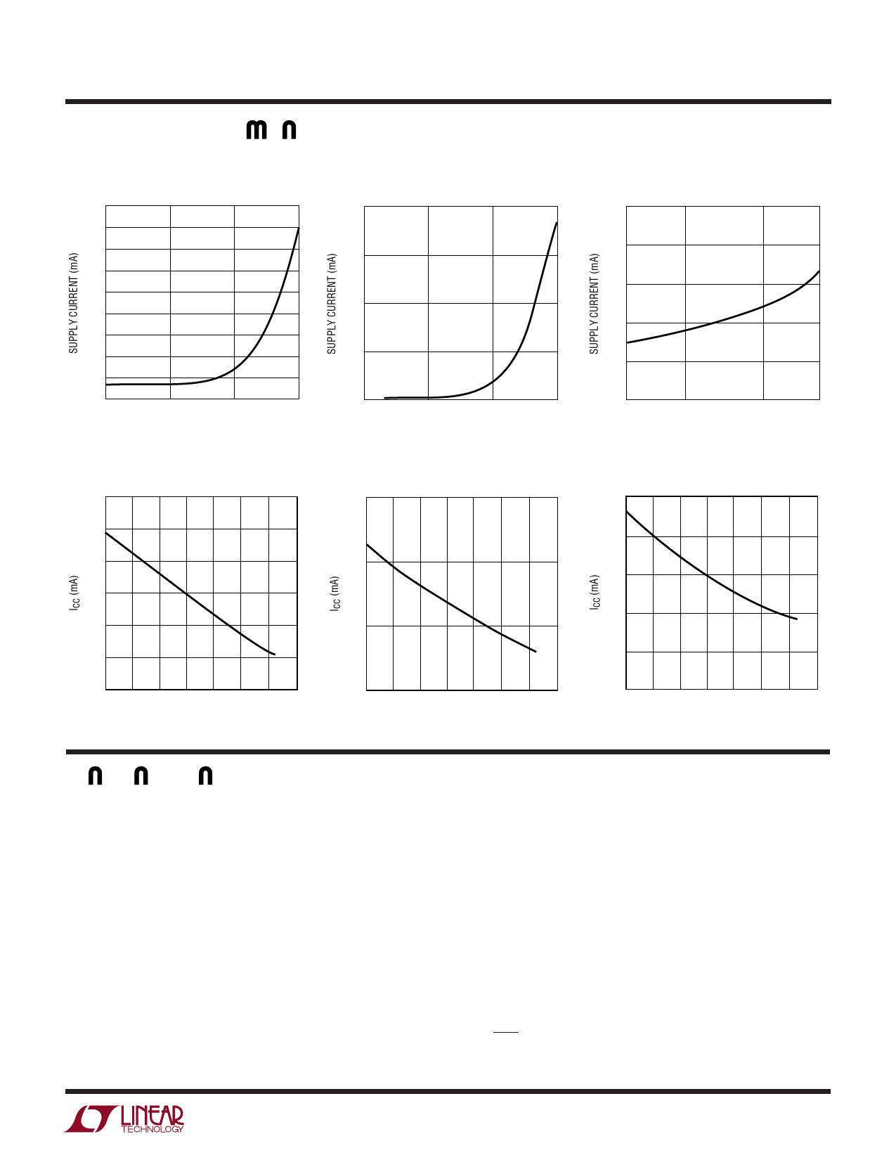
TYPICAL PERFOR A CE CHARACTERISTICS
V.11 Mode
Supply Current vs Data Rate
180
170
160
150
140
130
120
110
100
90
10
100
1000
DATA RATE (kBd)
10000
V.11 Mode
ICC vs Temperature
115
1546 • G01
V.35 Mode
Supply Current vs Data Rate
150
145
140
135
130
10
100
1000
DATA RATE (kBd)
V.35 Mode
ICC vs Temperature
140
10000
1546 • G02
110
105
135
100
95
130
90
85
–40 –20
0 20 40 60
TEMPERATURE (°C)
80 100
1546 • G04
125
–40 –20
0 20 40 60
TEMPERATURE (°C)
80 100
1546 • G05
V.28 Mode
Supply Current vs Data Rate
35
34
33
32
31
30
10
20
50
DATA RATE (kBd)
V.28 Mode
ICC vs Temperature
40
100
1546 • G03
38
36
34
32
30
–40 –20
0 20 40 60
TEMPERATURE (°C)
80 100
1546 • G06
PI FU CTIO S
C1–␣ (Pin 1): Capacitor C1 Negative Terminal. Connect a
1µF capacitor between C1+ and C1–.
C1+ (Pin 2): Capacitor C1 Positive Terminal. Connect a
1µF capacitor between C1+ and C1 –.
VDD (Pin 3): Generated Positive Supply Voltage for
V.28. Connect a 1µF capacitor to ground.
VCC (Pin 4): Positive Supply Voltage Input. 4.75V ≤ VCC
≤ 5.25V. Bypass with a 1µF capacitor to ground.
D1 (Pin 5): TTL Level Driver 1 Input.
D2 (Pin 6): TTL Level Driver 2 Input.
D3 (Pin 7): TTL Level Driver 3 Input.
R1 (Pin 8): CMOS Level Receiver 1 Output.
R2 (Pin 9): CMOS Level Receiver 2 Output.
R3 (Pin 10): CMOS Level Receiver 3 Output.
M0 (Pin 11): TTL Level Mode Select Input 0 with Pull-Up
to VCC. See Table 1.
M1 (Pin 12): TTL Level Mode Select Input 1 with Pull-Up
to VCC. See Table 1.
M2 (Pin 13): TTL Level Mode Select Input 2 with Pull-Up
to VCC. See Table 1.
DCE/DTE (Pin 14): TTL Level Mode Select Input with Pull-
Up to VCC. See Table 1.
5
Share Link: 