MC141524T1 View Datasheet(PDF) - Motorola => Freescale
Part Name
Description
Manufacturer
MC141524T1 Datasheet PDF : 12 Pages
| |||
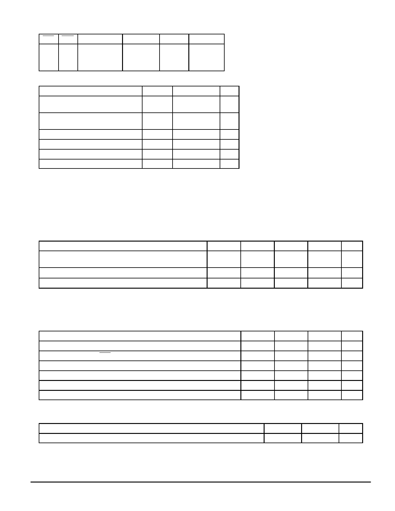
TRUTH TABLE FOR TAG AND DATA RAMs (X = Don’t Care)
COE CWE
Mode
VCC Current Output
Cycle
H
H Output Disabled
ICCA
L
H
Read
ICCA
X
L
Write
ICCA
High–Z
Dout
High–Z
—
Read Cycle
Write Cycle
ABSOLUTE MAXIMUM RATINGS
Rating
Symbol
Value
Unit
Power Supply Voltage
for Tag VCC5
– 0.5 to + 7.0
V
for Data VCC3
– 0.5 to + 5.0
Voltage Relative to VSS
Vin, Vout
– 0.5 to VCC
V
+ 0.5*
Output Current (per I/O)
Iout
± 20
mA
Temperature Under Bias
Tbias
– 10 to + 85
°C
Operating Temperature
TA
0 to + 70
°C
Storage Temperature – Plastic
Tstg
– 55 to + 125
°C
v * For data RAMs, VCC + 2.0 V ac to VSS – 2.0 V ac (pulse width 20 ns).
NOTE: Permanent device damage may occur if ABSOLUTE MAXIMUM RATINGS are
exceeded. Functional operation should be restricted to RECOMMENDED OPER-
ATING CONDITIONS. Exposure to higher than recommended voltages for ex-
tended periods of time could affect device reliability.
This device contains circuitry to protect the
inputs against damage due to high static volt-
ages or electric fields; however, it is advised
that normal precautions be taken to avoid
application of any voltage higher than maxi-
mum rated voltages to this high–impedance
circuit.
This CMOS memory circuit has been de-
signed to meet the dc and ac specifications
shown in the tables, after thermal equilibrium
has been established. The circuit is in a test
socket or mounted on a printed circuit board
and transverse air flow of at least 500 linear
feet per minute is maintained.
DC OPERATING CONDITIONS AND CHARACTERISTICS
(VCC3 = 3.3 V ± 5%, VCC5 = 5.0 V ± 5%, TA = 0 to + 70°C, Unless Otherwise Noted)
RECOMMENDED OPERATING CONDITIONS (Voltages Referenced to VSS = 0 V)
Parameter
Symbol
Min
Typ
Supply Voltage (Operating Voltage Range)
Tag RAM
VCC
4.75
5.0
Data RAM and Latch
3.135
3.3
Input High Voltage
VIH
2.2
—
Input Low Voltage
VIL
– 0.5**
0.0
* For Tag, VIH (max) = VCC + 0.3 V dc; VIH (max) = VCC + 2.0 V ac (pulse width ≤ 20 ns).
For Data, VIH (max) = VCC + 0.3 V dc; VIH (max) = VCC + 2.0 V ac (pulse width ≤ 10% tAVAV (min)).
** For Tag, VIL (min) = – 0.5 V dc; VIL (min) = – 2.0 V ac (pulse width ≤ 20 ns).
For Data, VIL (min) = – 0.5 V dc; VIL (min) = – 2.0 V ac (pulse width ≤ 10% tAVAV (min)).
Max
Unit
5.25
V
3.465
VCC + 0.3* V
0.8
V
DC CHARACTERISTICS
Parameter
Input Leakage Current (All Inputs, Vin = 0 to VCC)
Output Leakage Current (COE = VIH, Vout = 0 to VCC)
TTL Output Low Voltage (IOL = + 8.0 mA)
TTL Output High Voltage (IOH = – 4.0 mA)
CMOS Output Low Voltage (IOL = 100 µA)
CMOS Output High Voltage (IOH = – 100 µA)
NOTE: NOTE: Good decoupling of the local power supply should always be used.
Symbol
Min
Max
Unit
Ilkg(I)
—
Ilkg(O)
—
±2
µA
±2
µA
VOL
—
VOH
2.4
VOL2
—
0.4
V
—
V
0.1
V
VOH2
VCC – 0.1
—
V
POWER SUPPLY CURRENTS
Parameter
AC Active Supply Current (Iout = 0 mA, VCC = Max, f = fmax)
Symbol
ICCA
Max
Unit
780
mA
MOTOROLA FAST SRAM
MCM64AF32
5
Share Link: 