GS841E18AB-133I View Datasheet(PDF) - Giga Semiconductor
Part Name
Description
Manufacturer
GS841E18AB-133I Datasheet PDF : 29 Pages
| |||
GS841E18AT/B-166/150/130/100
Package Thermal Characteristics
Rating
Layer Board Symbol TQFP max PBGA max Unit Notes
Junction to Ambient (at 200 lfm)
Junction to Ambient (at 200 lfm)
Notes:
Junction to Case (TOP)
single
RΘJA
32
four
RΘJA
20
—
RΘJC
7
28
°C/W
1,2
18
°C/W
1,2
4
°C/W
3
1. Junction temperature is a function of SRAM power dissapation, package thermal resistance, mounting board temperature, ambient.
Temperature air flow, board density, and PCB thermal resistance.
2. SCMI G-38-87.
3. Average thermal resistance between die and top surface, MIL SPEC-883, Method 1012.1.
AC Test Conditions
(VDD = 3.135 V–3.6 V, TA = 0–70°C)
Parameter
Input high level
Input low level
Input slew rate
Input reference level
Output reference level
Output load
Conditions
VIH = 2.3 V
VIL = 0.2 V
TR = 1 V/ns
1.25 V
1.25 V
Fig. 1& 2
Notes:
1. Include scope and jig capacitance.
2. Test conditions as specified with output loading as shown in Fig. 1
unless otherwise noted.
3. Output load 2 for tLZ, tHZ, tOLZ and tOHZ.
4. Device is deselected as defined by the Truth Table.
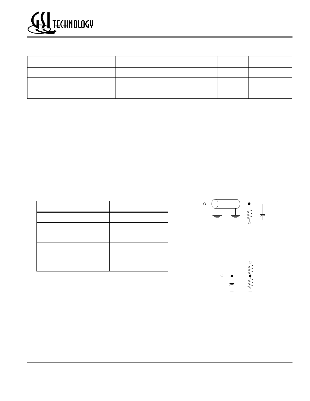
Output load 1
DQ
50W 30pF1
VT = 1.25 V
FIG. 1
Output load 2
2.5 V
DQ
225W
5pF1 225W
FIG. 2
Rev: 1.00 10/2001
10/29
© 2001, Giga Semiconductor, Inc.
Specifications cited are subject to change without notice. For latest documentation see http://www.gsitechnology.com.
Share Link: 