GS841E18AB-133I View Datasheet(PDF) - Giga Semiconductor
Part Name
Description
Manufacturer
GS841E18AB-133I Datasheet PDF : 29 Pages
| |||
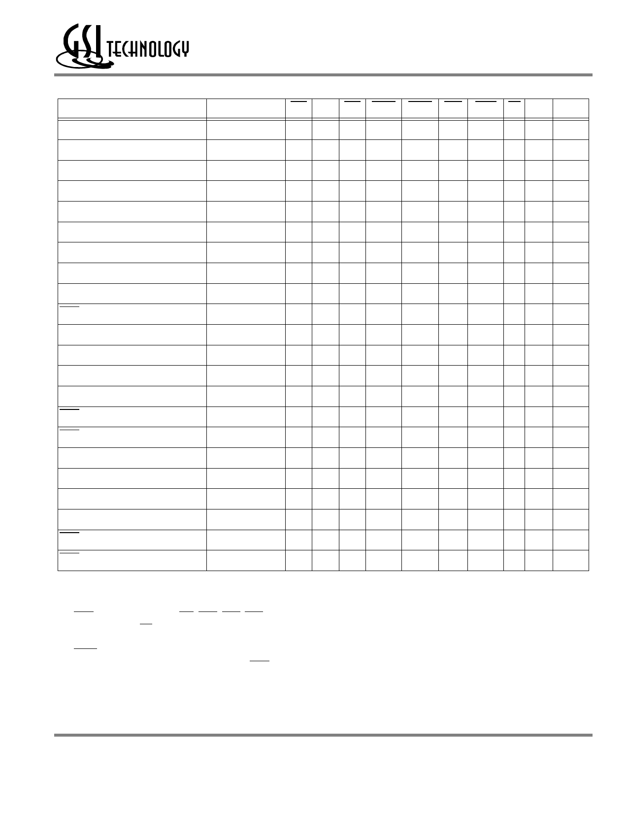
Synchronous Truth Table
Operation
Deselect Cycle, Power Down
Deselect Cycle, Power Down
Deselect Cycle, Power Down
Deselect Cycle, Power Down
Deselect Cycle, Power Down
Read Cycle, Begin Burst
Read Cycle, Begin Burst
Read Cycle, Begin Burst
Read Cycle, Begin Burst
Write Cycle, Begin Burst
Read Cycle, Continue Burst
Read Cycle, Continue Burst
Read Cycle, Continue Burst
Read Cycle, Continue Burst
Write Cycle, Continue Burst
Write Cycle, Continue Burst
Read Cycle, Suspend Burst
Read Cycle, Suspend Burst
Read Cycle, Suspend Burst
Read Cycle, Suspend Burst
Write Cycle, Suspend Burst
Write Cycle, Suspend Burst
GS841E18AT/B-166/150/130/100
Address Used
none
none
none
none
none
external
external
external
external
external
next
next
next
next
next
next
current
current
current
current
current
current
CE1 CE2 CE3 ADSP ADSC ADV Write OE CLK DQ
HXX
X
L
X
X X L-H High-Z
LLX
L
X
X
X X L-H High-Z
LXH
L
X
X
X X L-H High-Z
LLX
H
L
X
X X L-H High-Z
LXH
H
L
X
X X L-H High-Z
LHL
L
X
X
X L L-H Q
LHL
L
X
X
X H L-H High-Z
LHL
H
L
X
H L L-H Q
LHL
H
L
X
H H L-H High-Z
LHL
H
L
X
L X L-H D
XXX
H
H
L
H L L-H Q
XXX
H
H
L
H H L-H High-Z
HXX
X
H
L
H L L-H Q
HXX
X
H
L
H H L-H High-Z
XXX
H
H
L
L X L-H D
HXX
X
H
L
L X L-H D
XXX
H
H
H
H L L-H Q
XXX
H
H
H
H H L-H High-Z
HXX
X
H
H
H L L-H Q
HXX
X
H
H
H H L-H High-Z
XXX
H
H
H
L X L-H D
HXX
X
H
H
L X L-H D
Notes:
1. X means “don’t care,” H means “logic high,” L means “logic low.”
2. Write is the logic function of GW, BWE, BW1, BW2. See Byte Write Function table for detail.
3. All inputs, except OE, must meet setup and hold on rising edge of CLK.
4. Suspending busrt generates a wait cycle.
5. ADSP LOW along with SRAM being selected always initiates a Read cycle at the L-H edge of the clock (CLK).
6. A Write cycle can only be performed by setting Write low for the clock L-H edge of the subsequent wait cycle.
Refer to page 12 for the Write timing diagram.
Rev: 1.00 10/2001
8/29
© 2001, Giga Semiconductor, Inc.
Specifications cited are subject to change without notice. For latest documentation see http://www.gsitechnology.com.
Share Link: 