ICS9342YF-T View Datasheet(PDF) - Integrated Circuit Systems
Part Name
Description
Manufacturer
ICS9342YF-T Datasheet PDF : 10 Pages
| |||
ICS9342
General Description
The ICS9342 generates all clocks required for high speed PowerPC RISC microprocessor systems. With a zero delay buffer
chip such as the ICS9112-17 multiple PCI clock outputs can be generated in phase with PCIREF.
Spread Spectrum may be enabled by driving the SS_EN# pin low. Spread spectrum typically reduces system EMI by 8dB to
10dB. This simplifies EMI qualification without resorting to board design iterations or costly shielding. The ICS9342
employs a proprietary closed loop design, which tightly controls the percentage of spreading over process and temperature
variations.
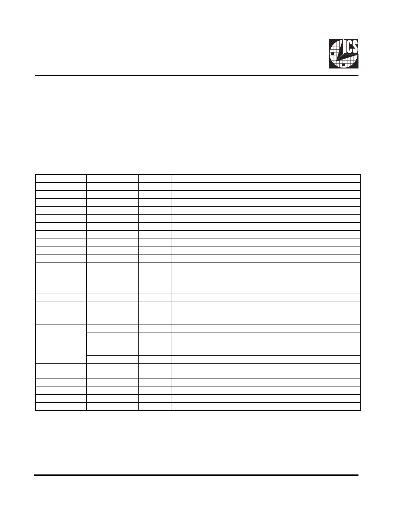
Pin Configuration
PIN NUMBER
1
2,3
4
5
6
7
8
9
10
11
12
13
14
15
18, 17, 16
19
20
21
22
23
24
48, 25
26, 31, 36, 41, 46
27, 32, 37, 42, 47
PIN NAME
VDDREF
R EF [1 :0]
GNDREF
X1
X2
PD#
CPU_STOP#
VDD
GND
P CI_S TO P #
SS_EN#
VDDPCI
PCIREF
GNDPCI
FS (2:0)
VDDFP
GNDFP
OUT
TEST#
O U T_D IV 2
BOOST#
PDFP#
VDDA
O U TS EL(1 :0 )
GNDCPU
VDDCPU
TYPE
PWR
OUT
PWR
IN
OUT
IN
IN
PWR
PWR
IN
IN
PWR
OUT
PWR
IN
PWR
PER
OUT
IN
OUT
IN
IN
PWR
IN
PWR
PWR
DESCRIPTION
Ref(1:0), XTAL power supply, nominal 3.3V
14.318 M Hz reference clocks
Ground pin for the REF outputs
Crystal input,nominally 14.318M Hz.
Crystal output, nominally 14.318M Hz.
Pow ers down chip, active low .
Stops all CPUCLKs [11:0] at logic 0 level, w hen input low
3.3V power for the digital core.
Ground pin for the digital core.
Drives PCIREF to logic 0 level, when input low
Spread spectrum is turned on by driving this input low and turned off by
driving it high.
Pow er supply for PCIREF, nominal 3.3V.
Reference clock for PCI Zero Delay Buffer.
Ground pin for PCIREF.
Frequency select pins.
3.3V power for the Fixed PLL core.
Ground pin for the Fixed PLL core.
3.3V O UT reference clock.
Logic input to select over clocking or under clocking frequencies.
(latched input)
3.3V 1/2 frequency OUT reference clock.
Logic input to select normal or test mode frequencies. (latched input)
Pow ers down Fixed PLL. When driven to low, OUT and OUT_DIV2 clocks
will be stopped
3.3V power for the PLL core
Frequency select pins for OUT and OUT_DIV2 clocks.
Ground pin for CPU clocks.
3.3V power supply for CPU clocks.
Third party brands and names are the property of their respective owners.
2
Share Link: 