CXD2424R View Datasheet(PDF) - Sony Semiconductor
Part Name
Description
Manufacturer
CXD2424R Datasheet PDF : 31 Pages
| |||
CXD2424R
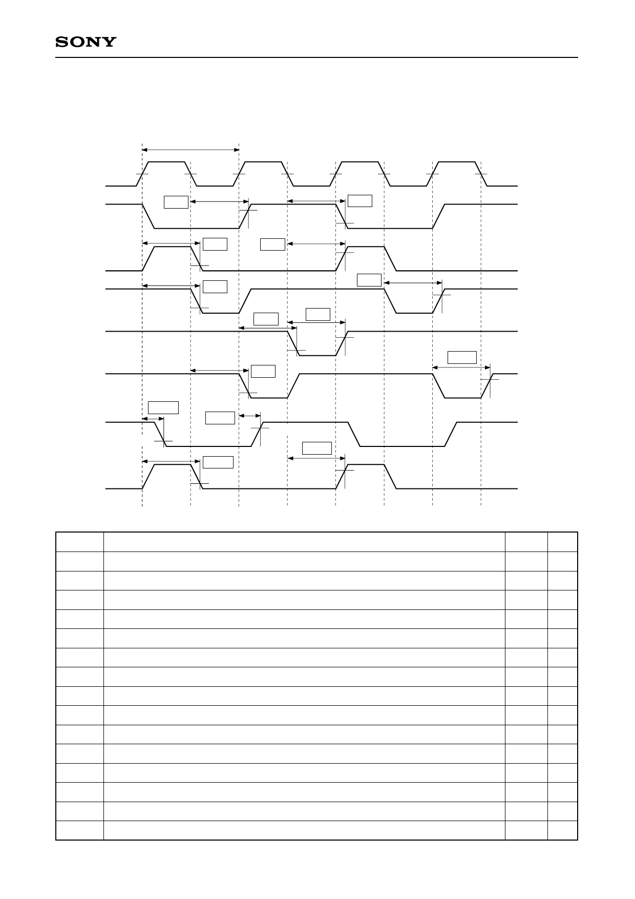
AC Characteristics
1) Phase characteristics of XH1, RG, XSHP, XSHD, XRS, CL, and CLD
tCK
CK
Vpp/2
XH1
RG
XSHP
XSHD
XRS
CL
CLD
tpd1
0.3VDD
0.3VDD
tpd11
0.3VDD
0.3VDD
0.7VDD
tpd3
tpd5
0.3VDD
tpd12
tpd13
tpd4
0.3VDD
0.7VDD
tpd7
0.3VDD
tpd9
tpd8
0.7VDD
tpd14
0.7VDD
tpd2
tpd6
0.7VDD
0.7VDD
tpd10
0.7VDD
(VDD = 5.0V, Topr = 25°C, Load capacity of CL and CLD = 30pF, Load capacity of XH1, XSHP, XSHD, XRS, and RG = 10pF)
Symbol
tCK
tpd1
tpd2
tpd3
tpd4
tpd5
tpd6
tpd7
tpd8
tpd9
tpd10
tpd11
tpd12
tpd13
tpd14
Definition
CK cycle
XH1 rising delay, activated by the falling edge of CK
XH1 falling delay, activated by the falling edge of CK
RG falling delay, activated by the rising edge of CK
RG rising delay, activated by the falling edge of CK
XSHP falling delay, activated by the rising edge of CK
XSHP rising delay, activated by the falling edge of CK
XSHD falling delay, activated by the rising edge of CK
XSHD rising delay, activated by the falling edge of CK
XRS falling delay, activated by the falling edge of CK
XRS rising delay, activated by the rising edge of CK
CL falling delay, activated by the rising edge of CK
CL rising delay, activated by the rising edge of CK
CLD falling delay, activated by the rising edge of CK
CLD rising delay, activated by the falling edge of CK
Typ. Unit
35 ns
8
ns
9
ns
11 ns
15 ns
18 ns
18 ns
20 ns
11 ns
17 ns
15 ns
32 ns
0
ns
26 ns
20 ns
–7–
Share Link: 