NC7S04CW View Datasheet(PDF) - Fairchild Semiconductor
Part Name
Description
Manufacturer
NC7S04CW Datasheet PDF : 7 Pages
| |||
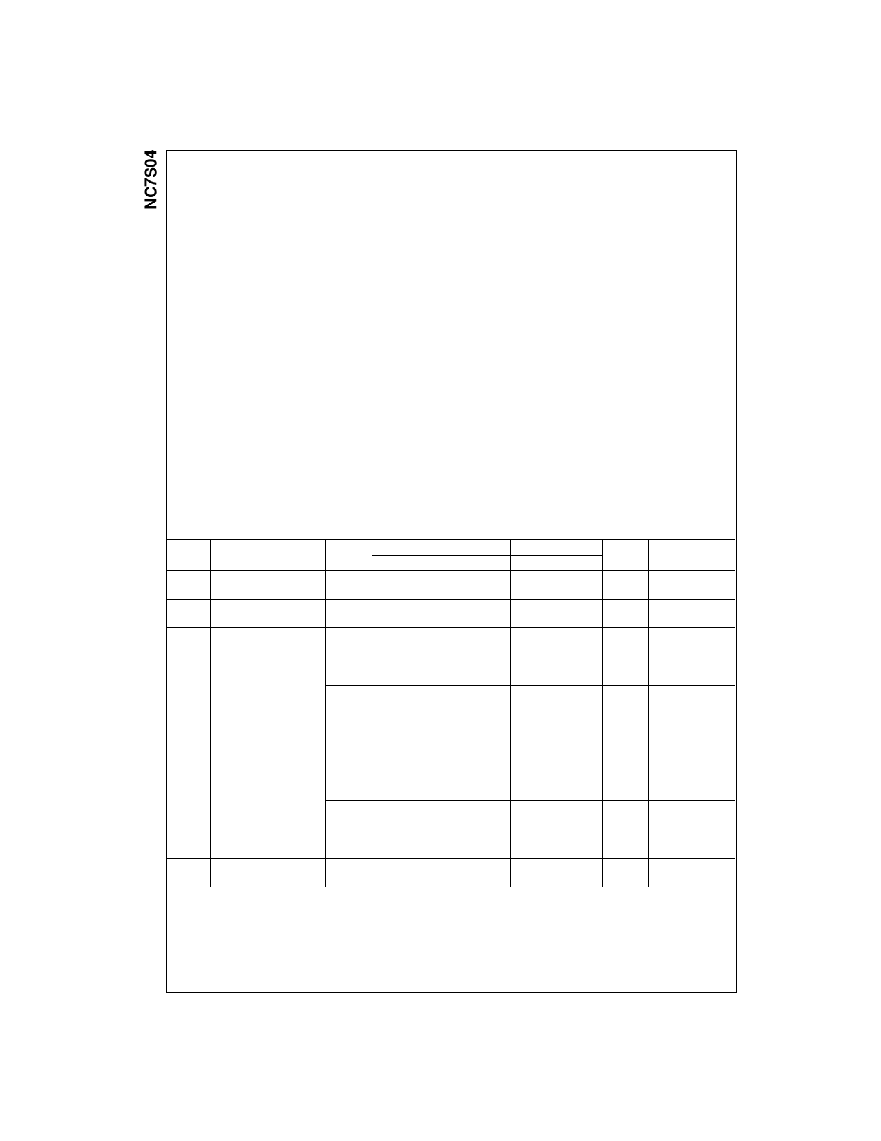
Absolute Maximum Ratings(Note 1)
Supply Voltage (VCC)
DC Input Diode Current (IIK)
@VIN ≤ −0.5V
@VIN ≥ VCC + 0.5V
DC Input Voltage (VIN)
DC Output Diode Current (IOK)
@VOUT ≤ −0.5V
@VOUT ≥ VCC + 0.5V
DC Output Voltage (VOUT)
DC Output Source or Sink
Current (IOUT)
DC VCC or Ground Current per
Output Pin (ICC or IGND)
Storage Temperature (TSTG)
Junction Temperature (TJ)
Lead Temperature (TL)
(Soldering, 10 seconds)
Power Dissipation (PD) @ +85°C
SOT23-5
SC70-5
−0.5V to +7.0V
−20 mA
+20 mA
−0.5V to VCC +0.5V
−20 mA
+20 mA
−0.5V to VCC +0.5V
±12.5 mA
±25 mA
−65°C to +150°C
150°C
260°C
200 mW
150 mW
Recommended Operating
Conditions (Note 2)
Supply Voltage (VCC)
Input Voltage (VIN)
Output Voltage (VOUT)
Operating Temperature (TA)
Input Rise and Fall Time (tr, tf)
VCC @ 2.0V
VCC @ 3.0V
VCC @ 4.5V
VCC @ 6.0V
Thermal Resistance (θJA)
SOT23-5
SC70-5
2.0V to 6.0V
0V to VCC
0V to VCC
−40°C to +85°C
0 to 1000 ns
0 to 750 ns
0 to 500 ns
0 to 400 ns
300°C/W
425°C/W
Note 1: Absolute maximum ratings are those values beyond which damage
to the device may occur. The databook specifications should be met, with-
out exception, to ensure that the system design is reliable over its power
supply, temperature, and output/input loading variables. Fairchild does not
recommend operation of circuits outside the databook specifications.
Note 2: Unused inputs must be held HIGH or LOW. They may not float.
DC Electrical Characteristics
Symbol
Parameter
VIH
HIGH Level Input Voltage
VIL
LOW Level Input Voltage
VOH
HIGH Level Output Voltage
VCC
(V)
2.0
3.0–6.0
2.0
3.0–6.0
2.0
3.0
4.5
6.0
TA = +25°C
Min
Typ
Max
1.50
0.7 VCC
0.50
1.90
0.3 VCC
2.0
2.90
3.0
4.40
4.5
5.90
6.0
TA = −40°C to +85°C
Min
Max
1.50
0.7 VCC
0.50
1.90
0.3 VCC
2.90
4.40
5.90
3.0
4.5
6.0
VOL
LOW Level Output Voltage
2.0
3.0
4.5
6.0
2.68
2.85
2.63
4.18
4.35
4.13
5.68
5.85
5.63
0.0
0.10
0.10
0.0
0.10
0.10
0.0
0.10
0.10
0.0
0.10
0.10
3.0
4.5
6.0
IIN
Input Leakage Current
6.0
ICC
Quiescent Supply Current
6.0
0.1
0.26
0.33
0.1
0.26
0.33
0.1
0.26
0.33
±0.1
±1.0
1.0
10.0
Units
V
V
Conditions
V
IOH = −20 µA
VIN = VIL
VIN = VIL
V
IOH = −1.3 mA
IOH = −2 mA
IOH = −2.6 mA
V
IOL = 20 µA
VIN = VIH
VIN = VIH
V
IOL = 1.3 mA
IOL = 2 mA
IOL = 2.6 mA
µA
VIN = VCC,GND
µA
VIN = VCC, GND
www.fairchildsemi.com
2
Share Link: 