SSTVN16857 View Datasheet(PDF) - Fairchild Semiconductor
Part Name
Description
Manufacturer
SSTVN16857 Datasheet PDF : 7 Pages
| |||
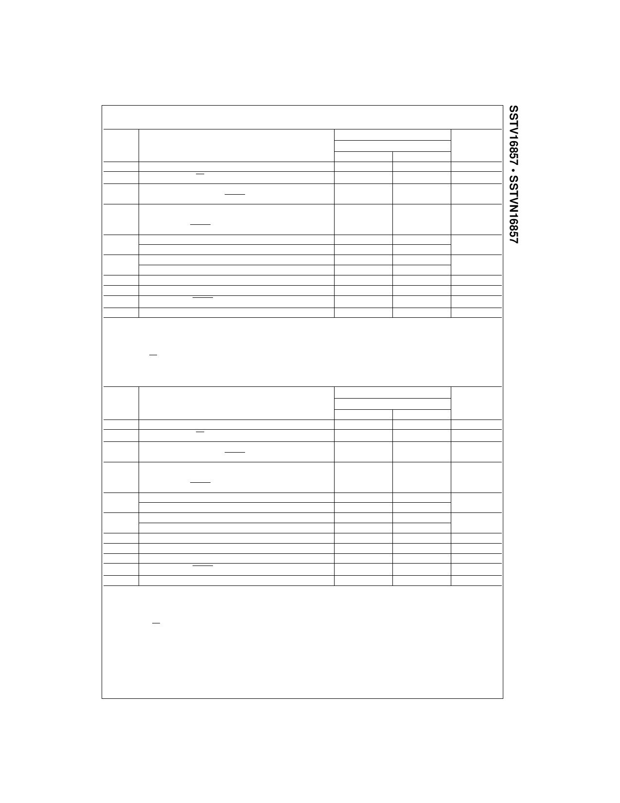
AC Electrical Characteristics (SSTV16857) (Note 4)
Symbol
Parameter
fMAX
Maximum Clock Frequency
tW
tACT
(Note 5)
Pulse Duration, CK, CK HIGH or LOW (Figure 2)
Differential Inputs Activation Time,
data inputs must be LOW after RESET HIGH (Figure 3)
tINACT
(Note 5)
Differential Inputs De-activation Time,
data and clock inputs must be held at valid levels
(not floating) after RESET LOW
tS
Setup Time, Fast Slew Rate (Note 6)(Note 7) (Figure 5)
Setup Time, Slow Slew Rate (Note 7)(Note 8) (Figure 5)
tH
Hold Time, Fast Slew Rate (Note 6)(Note 8) (Figure 5)
Hold Time, Slow Slew Rate (Note 7)(Note 8) (Figure 5)
tREM
tPHL, tPLH
Reset Removal Time (Figure 7)
Propagation Delay CLK, CLK to Qn (Figure 4)
tPHL
Propagation Delay RESET to Qn (Figure 6)
tSK(Pn-Pn) Output to Output Skew
Note 4: Refer to Figure 1 through Figure 7.
Note 5: This parameter is not production tested.
Note 6: For data signal input slew rate t 1 V/ns.
Note 7: For data signal input slew rate t 0.5 V/ns and 1 V/ns.
Note 8: For CK, CK signals input slew rates are t 1 V/ns.
TA 0qC to 70qC, CL 30 pF, RL 50:
VDD 2.5V r 0.2V; VDDQ 2.5V r 0.2V
Min
Max
200
2.5
22
22
0.65
0.9
0.75
0.9
10
1.1
2.8
5.0
200
AC Electrical Characteristics (SSTVN16857) (Note 9)
Symbol
Parameter
fMAX
Maximum Clock Frequency
tW
tACT
(Note 5)
Pulse Duration, CK, CK HIGH or LOW (Figure 2)
Differential Inputs Activation Time,
data inputs must be LOW after RESET HIGH (Figure 3)
tINACT
(Note 5)
Differential Inputs De-activation Time,
Data and Clock Inputs must be held at valid levels
(not floating) after RESET LOW
tS
Setup Time, Fast Slew Rate (Note 9)(Note 12) (Figure 5)
Setup Time, Slow Slew Rate (Note 12)(Note 13) (Figure 5)
tH
Hold Time, Fast Slew Rate (Note 11)(Note 13) (Figure 5)
Hold Time, Slow Slew Rate (Note 12)(Note 13) (Figure 5)
tREM
tPHL, tPLH
tPSS
Reset Removal Time (Figure 7)
Propagation Delay CLK, CLK to Qn (Figure 4)
Propagation Delay Simultaneous Switching CLK, CLK to Qn (Note 14)
tPHL
Propagation Delay RESET to Qn (Figure 6)
tSK(Pn-Pn) Output to Output Skew
Note 9: Refer to Figure 1 through Figure 7.
Note 10: This parameter is not production tested.
Note 11: For data signal input slew rate t 1 V/ns.
Note 12: For data signal input slew rate t 0.5 V/ns and 1 V/ns.
Note 13: For CK, CK signals input slew rates are t 1 V/ns.
Note 14: Simultaneous Switching is guaranteed by characterization.
TA 0qC to 70qC, CL 30 pF, RL 50:
VDD 2.5V r 0.2V; VDDQ 2.5V r 0.2V
Min
Max
220
2.5
22
22
0.65
0.75
0.75
0.9
10
1.1
2.4
2.7
5.0
200
Units
MHz
ns
ns
ns
ns
ns
ns
ns
ns
ps
Units
MHz
ns
ns
ns
ns
ns
ns
ns
ns
ns
ps
5
www.fairchildsemi.com
Share Link: 