AD6644 View Datasheet(PDF) - Analog Devices
Part Name
Description
Manufacturer
AD6644 Datasheet PDF : 24 Pages
| |||
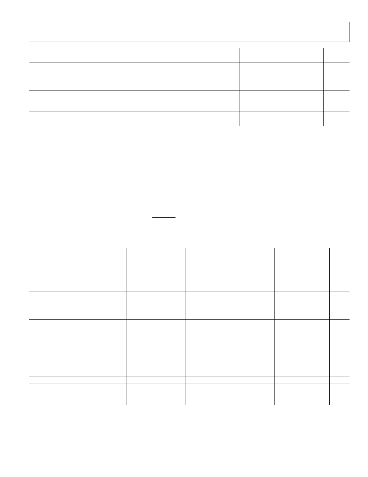
AD6644
Parameter
DATA READY (DRY6)/DATA, OVR
Data Ready to DATA Delay (Hold Time)3
Encode = 65 MSPS (50% Duty Cycle)
Encode = 40 MSPS (50% Duty Cycle)
Data Ready to DATA Delay (Setup Time)3
@ 65 MSPS (50% Duty Cycle)
@ 40 MSPS (50% Duty Cycle)
APERTURE DELAY
APERTURE UNCERTAINTY (JITTER)
Name
tH_DR
tS_DR
tA
tJ
Temp Test Level1
Full
IV
Full
IV
Full
IV
Full
IV
25°C
V
25°C
V
AD6644AST-40/65
Min
Typ
Max
See note7
8.0
8.6
9.4
12.8
13.4
14.2
See note7
3.2
5.5
6.5
8.0
10.3
11.3
100
0.2
Unit
ns
ns
ns
ns
ps
ps rms
1 See the Explanation of Test Levels section.
2 Several timing parameters are a function of tENC and tENCH.
3 To compensate for a change in duty cycle for tH_DR and tS_DR use the following equations:
NewtH_DR = (tH_DR − % Change(tENCH)) × tENC/2
NewtS_DR = (tS_DR − % Change(tENCH)) × tENC/2
4 ENCODE to data delay (hold time) is the absolute minimum propagation delay through the ADC.
5 ENCODE to data delay (setup time) is calculated relative to 65 MSPS (50% duty cycle). To calculate tS_E for a given encode, use the following equation:
NewtS_E = tENC(NEW) − tENC + tS_E (that is, for 40 MSPS, NewtS_E(TYP) = 25 × 10−9 − 15.38 × 10⁻⁹ + 9.8 × 10−9 = 19.4 × 10⁻⁹).
6 DRY is an inverted and delayed version of the encode clock. Any change in the duty cycle of the clock correspondingly changes the duty cycle of DRY.
7 Data ready to data delay (tH_DR and tS_DR) is calculated relative to 65 MSPS (50% duty cycle) and is dependent on tENC and duty cycle. To calculate tH_DR and tS_DR for a
given encode, use the following equations:
NewtH_DR = tENC(NEW)/2 − tENCH + tH_DR (that is, for 40 MSPS, NewtH_DR(TYP) = 12.5 × 10⁻⁹ − 7.69 × 10⁻⁹ + 8.6 × 10−9 = 13.4 × 10⁻⁹).
NewtS_DR = tENC(NEW)/2 − tENCH + tS_DR (that is, for 40 MSPS, NewtS_DR(TYP) = 12.5 × 10⁻⁹ − 7.69 × 10⁻⁹ + 5.5 × 10−9 = 10.3 × 10⁻⁹).
AC SPECIFICATIONS
All ac specifications tested by driving ENCODE and ENCODE differentially.
AVCC = 5 V, DVCC = 3.3 V; ENCODE and ENCODE = maximum conversion rate MSPS; TMIN = −25°C, TMAX = +85°C, unless otherwise noted.
Table 5.
Parameter
SNR
Analog Input
@ −1 dBFS
SINAD2
Analog Input
@ −1 dBFS
WORST HARMONIC (2ND or 3RD)2
Analog Input
@ −1 dBFS
WORST HARMONIC (4TH or Higher)2
Analog Input
@ −1 dBFS
TWO-TONE SFDR2, 3, 4
TWO-TONE IMD REJECTION2, 4
F1, F2 @ −7 dBFS
ANALOG INPUT BANDWIDTH
Conditions
2.2 MHz
15.5 MHz
30.5 MHz
2.2 MHz
15.5 MHz
30.5 MHz
2.2 MHz
15.5 MHz
30.5 MHz
2.2 MHz
15.5 MHz
30.5 MHz
AD6644AST-40
AD6644AST-65
Temp Test Level1 Min Typ Max Min Typ Max Unit
25°C V
25°C II
25°C II
74.5
74.5
dB
74.0
72 74.0
dB
73.5
72 73.5
dB
25°C V
25°C II
25°C V
74.5
74.5
dB
74.0
72 74.0
dB
73.0
73.0
dB
25°C V
25°C II
25°C V
92
92
dBc
90
83 90
dBc
85
85
dBc
25°C V
25°C II
25°C V
Full
V
93
93
dBc
92
85 92
dBc
92
92
dBc
100
100
dBFS
Full
V
25°C V
90
90
dBc
250
250
MHz
1 See the Explanation of Test Levels section.
2 AVCC = 5 V to 5.25 V for rated ac performance.
3 Analog input signal power swept from −7 dBFS to −100 dBFS.
4 F1 = 15 MHz, F2 = 15.5 MHz.
Rev. D | Page 5 of 24
Share Link: 