AD6644 View Datasheet(PDF) - Analog Devices
Part Name
Description
Manufacturer
AD6644 Datasheet PDF : 24 Pages
| |||
AD6644
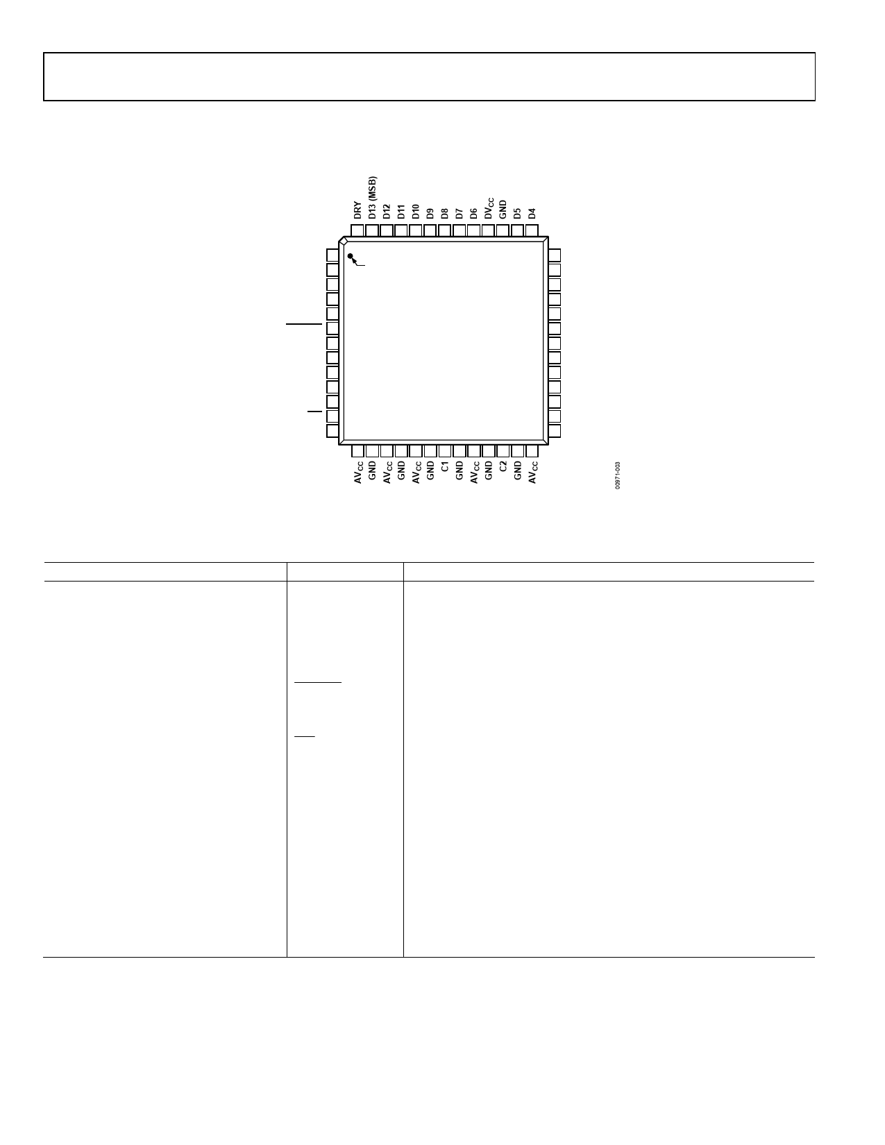
PIN CONFIGURATION AND FUNCTION DESCRIPTIONS
52 51 50 49 48 47 46 45 44 43 42 41 40
DVCC 1
GND 2
VREF 3
GND 4
ENCODE 5
ENCODE 6
GND 7
AVCC 8
AVCC 9
GND 10
AIN 11
AIN 12
GND 13
PIN 1
IDENTIFIER
AD6644
TOP VIEW
(Not to Scale)
39 D3
38 D2
37 D1
36 D0 (LSB)
35 DMID
34 GND
33 DVCC
32 OVR
31 DNC
30 AVCC
29 GND
28 AVCC
27 GND
DNC = DO NOT CONNECT 14 15 16 17 18 19 20 21 22 23 24 25 26
Figure 3. Pin Configuration
Table 8. Pin Function Descriptions
Pin Number
1, 33, 43
2, 4, 7, 10, 13, 15, 17, 19, 21, 23, 25, 27, 29,
34, 42
3
Mnemonic
DVCC
GND
VREF
5
6
8, 9, 14, 16, 18, 22, 26, 28, 30
11
12
20
ENCODE
ENCODE
AVCC
AIN
AIN
C1
24
C2
31
32
35
36
37 to 41, 44 to 50
51
52
DNC
OVR
DMID
D0 (LSB)
D1 to D5, D6 to
D12
D13 (MSB)
DRY
Description
3.3 V Power Supply (Digital), Output Stage Only.
Ground.
2.4 V (Analog Reference). Bypass to ground with 0.1 μF microwave chip
capacitor.
Encode Input. Conversion initiated on rising edge.
Complement of ENCODE. Differential input.
5 V Analog Power Supply.
Analog Input.
Complement of AIN. Differential analog input.
Internal Voltage Reference. Bypass to ground with 0.1 μF microwave chip
capacitor.
Internal Voltage Reference. Bypass to ground with 0.1 μF microwave chip
capacitor.
Do not connect this pin.
Overrange Bit. High indicates analog input exceeds ±FS.
Output Data Voltage Midpoint. Approximately equal to DVCC/2.
Digital Output Bit (Least Significant Bit). Twos complement.
Digital Output Bits in Twos Complement.
Digital Output Bit (Most Significant Bit). Twos complement.
Data Ready Output.
Rev. D | Page 8 of 24
Share Link: 