TDA4886A View Datasheet(PDF) - Philips Electronics
Part Name
Description
Manufacturer
TDA4886A Datasheet PDF : 52 Pages
| |||
Philips Semiconductors
140 MHz video controller with I2C-bus
Product specification
TDA4886A
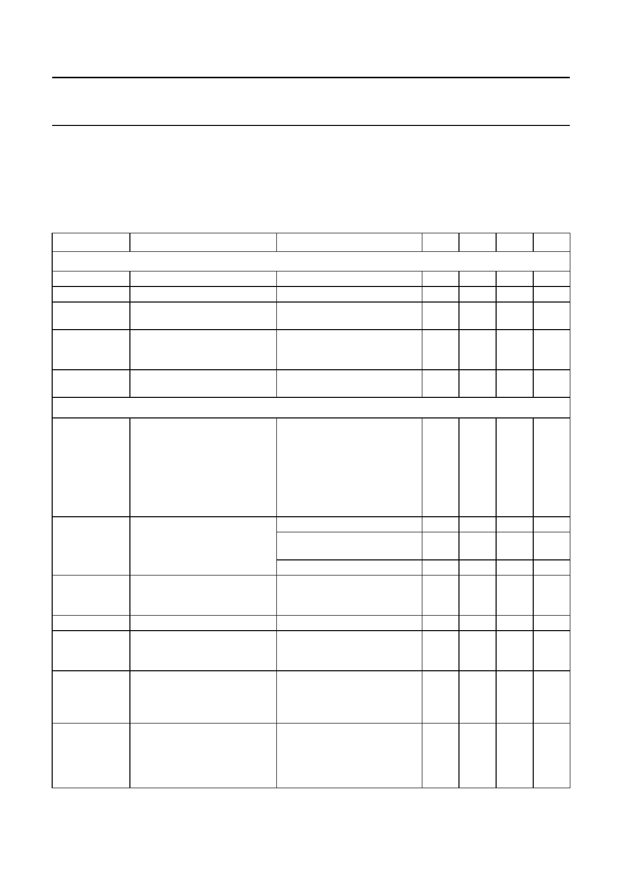
10 CHARACTERISTICS
All voltages and currents are measured in a dedicated test circuit which is optimized for best high frequency
performance; all voltages are measured with respect to GND (pins 9 and 14); VP = VP1, 2, 3 = 8 V (pins 7, 21,
18 and 15); Tamb = 25 °C; nominal input signals [0.7 V (p-p) at pins 6, 8 and 10]; nominal colour signals at signal
outputs (pins 22, 19 and 16); reference black level (Vrbl) approximately 0.77 V; nominal settings for brightness and
contrast; maximum settings for OSD contrast and gain; no subcontrast, modulation of contrast or limiting (V24 ≥ 5 V);
no OSD fast blanking (pin 1 connected to ground); notes 1 to 3; unless otherwise specified.
SYMBOL
PARAMETER
CONDITIONS
MIN. TYP. MAX. UNIT
Supplies
VP
IP
VP1,2,3
IP1,2,3
VPSO
supply voltage (pin 7)
supply current (pin 7)
channel supply voltage
(pins 21, 18 and 15)
channel supply current
(pins 21, 18 and 15)
supply voltage for signal switch
off (threshold at pin 7)
note 4
signal outputs (pins 22,
19 and 16) open-circuit;
Vrbl ≈ 0.77 V; notes 4 and 5
signal outputs switched to
switch-off voltage
7.6 8.0 8.8 V
−
21
25
mA
7.6 8.0 8.8 V
−
21
25
mA
−
−
7.2 V
Input clamping and vertical blanking input, validation of buffered I2C-bus data (pin 5)
V5
input clamping and vertical
notes 6 and 7
blanking input signal
no vertical blanking,
−0.1 −
no input clamping
vertical blanking,
no input clamping
1.6 −
input clamping,
no vertical blanking
3.5 −
I5
input current
V5 = 1 V
pin 5 connected to ground;
note 8
−
−0.2
−80 −60
V5 = −0.1 V; note 8
−250 −200
tr/f5
rise/fall time for input clamping note 6; see Fig.7
pulse, disable for vertical
−
−
blanking
tW5
tW5I2C
tI2Cvalid
tI2Cdead
width of input clamping pulse
0.6 −
width of vertical blanking pulse leading and trailing edge
10
−
for validation of buffered
I2C-bus data
threshold V5 = 1.4 V; note 7
delay between leading edge of I2C-bus transmission in
−
−
vertical blanking pulse and
buffered mode completed;
validation of buffered I2C-bus leading edge threshold
data
dead time of I2C-bus receiver
after synchronizing vertical
blanking pulse in case of a
completed I2C-bus transmission
V5 = 1.4 V; note 7
leading edge threshold
V5 = 1.4 V; note 7
15
−
in buffered mode
+1.2
2.6
VP
−
−30
−100
75
−
−
2
−
V
V
V
µA
µA
µA
ns/V
µs
µs
µs
µs
1998 Dec 04
11
Share Link: 