L9935 View Datasheet(PDF) - STMicroelectronics
Part Name
Description
Manufacturer
L9935 Datasheet PDF : 29 Pages
| |||
Functional description
L9935
5.13.1
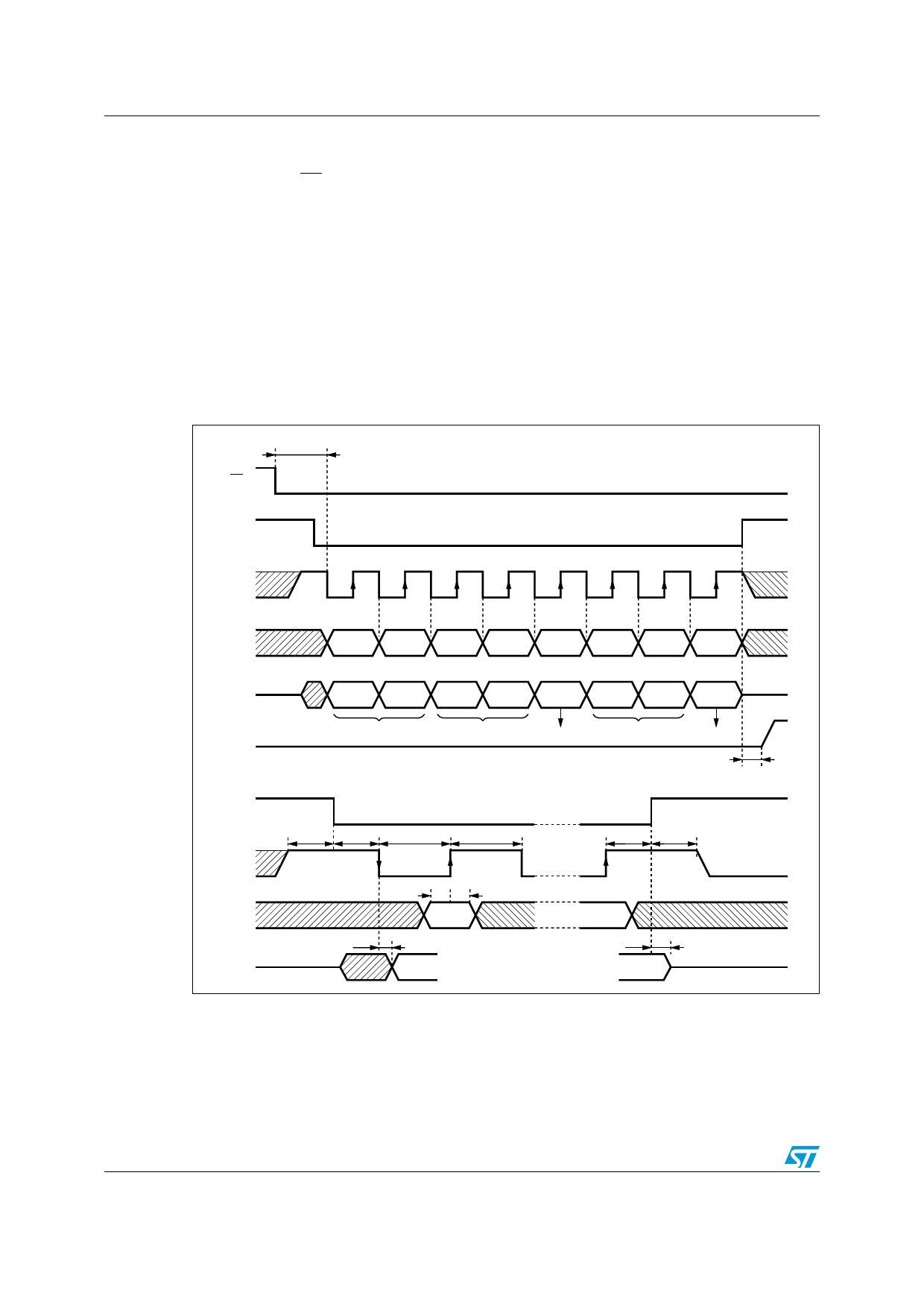
Startup of the serial data interface
Falling slope of EN activates the device. After ten.sck the device is ready to work.
Falling slope of CSN indicates start of frame. Data transfer (reading SDI into the register)
takes place at the rising slopes of SCK.
Data transfer of the register to SDO takes place at the falling slope of SCK.
Rising slope of CSN indicates end of frame. At the end of frame data will only be accepted if
modulo 8 bit (modulo 8 falling slopes to SCK) have been transferred. If this is not the case
the input will be ignored and the bridges will maintain the same status as before.
SDO is a tristate output.
SDO is active while CSN = LOW, while CSN = HIGH SDO is high resistive.
Figure 9.
SPI data/clock timing
TEN?SCK
%.
#3.
3#+
3$)
3$/
!8
#3.
3#+
3$)
3$/
-3"
BIT
BIT
BIT
BIT
BIT
BIT
BIT
-3"
BIT
%22/2�")43
BIT
BIT
BIT
BIT
BIT
BIT
#522%.4�!
0/,!2)49�!
#522%.4�" 0/,!2)49�"
T0D
T
T
TD
TCL
TCH
TSU TSH
BIT
BIT
T
T
BIT
TZCH
BIT
'!0'03
20/29
Doc ID 5198 Rev 10
Share Link: 