PC910X View Datasheet(PDF) - Sharp Electronics
Part Name
Description
Manufacturer
PC910X Datasheet PDF : 5 Pages
| |||
PC910X
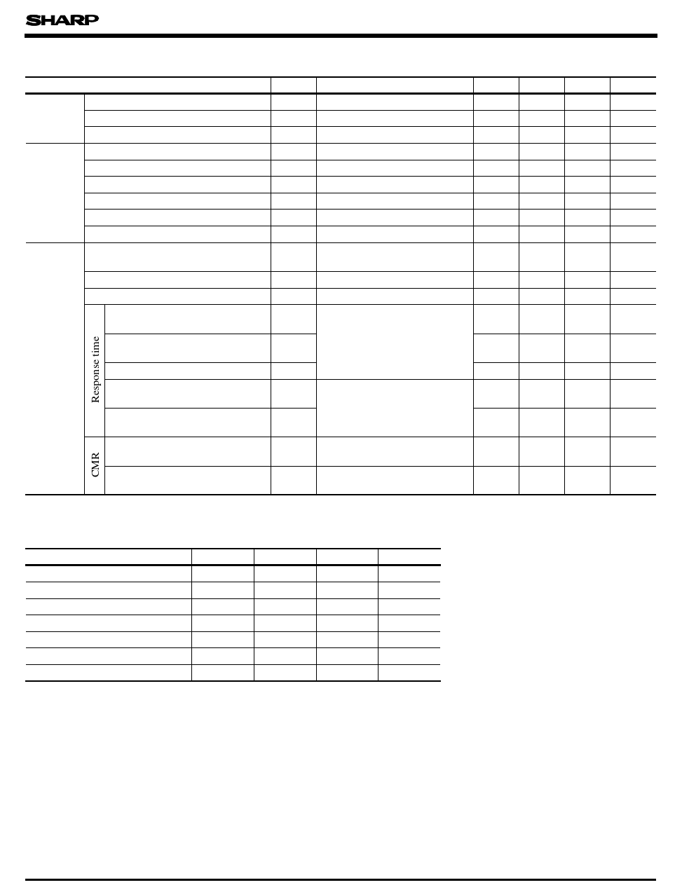
s Electro-optical Characteristics
Input
Output
Transfer
charac-
teristics
Parameter
Forward voltage
Reverse current
Terminal capacitance
High level output current
Low level output voltage
High level enable current
Low level enable current
High level supply current
Low level supply current
“ High→Low ” threshold
input current
Isolation resistance
Floating capacitance
“ High→Low” propagation
delay time
“ Low→High” propagation
delay time
Rise time, Fall time
“ High→Low” enable
propagation delay time
“ Low→High” enable
propagation delay time
Instantaneous common
mode rejection voltage
“ Output : High level ”
Instantaneous common
mode rejection voltage
“ Output : Low level ”
( Unless otherwise specified, Ta = 0 to 70˚C )
Symbol
Conditions
MIN.
V F Ta = 25˚C, I F = 10mA
-
IR Ta = 25˚C, VR = 5V
-
Ct Ta = 25˚C, V = 0, f = 1MH Z
-
I OH VCC = VO = 5.5V, V E = 2.0V, I F = 250 µ A
-
V OL VCC = 5.5V, V E = 2.0V, I F = 5mA, I OL = 13mA
-
I EH V CC = 5.5V, VE = 2.0V
-
IEL V CC = 5.5V, VE = 0.5V
-
I CCH VCC = 5.5V, I F = 0, VE = 0.5V
-
ICCL VCC = 5.5V, I F = 10mA, VE = 0.5V
-
I FHL
VCC = 5V, VE = 2.0V
VO = 0.8V, R L = 350 Ω
R iso Ta = 25˚C, DC500V, 40 to 60% RH
-
5 x 10¹⁰
Cf
t PHL
t PLH
tr , tf
t EHL
t ELH
CM H
CML
Ta = 25˚C, V = 0, f = 1MH Z
Fig. 1
Ta = 25˚C, VCC = 5V
RL = 350 Ω , C L = 15PF
IF = 7.5mA
Ta = 25˚C, VCC = 5V
Fig. 2
RL = 350 Ω, C L = 15pF
IF = 7.5mA, VEH = 3V
VEL = 0.5V
Ta = 25˚C, VCC = 5V, VCM = 10V(peak ) Fig. 3
RL = 350 Ω, I F = 0, V O(MIN ) = 2V
Ta = 25˚C, VCC = 5V, V CM = 10V(peak)
Fig. 3
RL = 350 Ω, I F = 5mA VO(MAX) = 0.8V
-
-
-
-
-
-
100
- 100
TYP.
1.6
-
60
2
0.4
- 0.8
- 1.2
7
13
2.5
1010
0.6
50
50
30
15
65
500
- 500
MAX. Unit
1.9
V
10
µA
150
PF
250
µA
0.6
V
- 1.8 mA
- 2.0 mA
15
mA
18
mA
5
mA
-
Ω
5
pF
120
ns
120
ns
60
ns
50
ns
100
ns
-
V/ µ s
-
V/ µ s
All typical values : at Ta = 25˚C, VCC = 5V
s Recommended Operating Conditions
Parameter
Low level input current
High level input current
High level enable voltage
Low level enable voltage
Supply voltage
Fanout ( TTL load )
Operating temperature
Symbol
MIN.
MAX.
Unit
I FL
0
250
µA
I FH
7
15
mA
V EH
2.0
V CC
V
V EL
0
0.8
V
V CC
4.5
5.5
V
N
-
8
-
T opr
0
70
˚C
1. When the enable input is in high level state, extemal pull-up resistor is
unnecessary.
2. Connect a by-pass ceramic capacitor ( 0.01 to 0.1µF) between
VCC and GND at the position within 1cm from pin.
Share Link: 