LTC1440(RevC) View Datasheet(PDF) - Linear Technology
Part Name
Description
Manufacturer
LTC1440 Datasheet PDF : 16 Pages
| |||
LTC1440/LTC1441/LTC1442
APPLICATIONS INFORMATION
LTC1440/LTC1441/LTC1442 are a family of micropower
comparators with built-in 1.182V reference. Features
include programmable hysteresis (LTC1440/LTC1442),
wide supply voltage range (2V to 11V) and the ability of the
reference to drive up to a 0.01µF capacitor without oscil-
lation. The comparators’ CMOS outputs can source up to
40mA and the supply current glitches, that normally occur
when switching logic states, have been eliminated.
Power Supplies
The comparator family operates from a single 2V to 11V
supply. The LTC1440 includes a separate ground for the
comparator output stage, allowing a split supply ranging
from ±1V to ±5.5V. Connecting V – to GND on the LTC1440
will allow single supply operation. If the comparator out-
put is required to source more than 1mA, or the supply
source impedance is high, V + should be bypassed with a
0.1µF capacitor.
Comparator Inputs
The comparator inputs can swing from the negative sup-
ply V – to within 1.3V max of the positive supply V +. The
inputs can be forced 300mV below V – or above V + without
damage and the typical input leakage current is only
±10pA.
capacitor of up to 0.01µF without oscillation and by
inserting a series resistor, capacitance values up to 100µF
can be used (Figure 1).
Figure 2 shows the resistor value required for different
capacitor values to achieve critical damping. Bypassing
the reference can help prevent false tripping of the com-
parators by preventing glitches on V + or reference load
transients from disturbing the reference output voltage.
Figure 3 shows the bypassed reference output with a
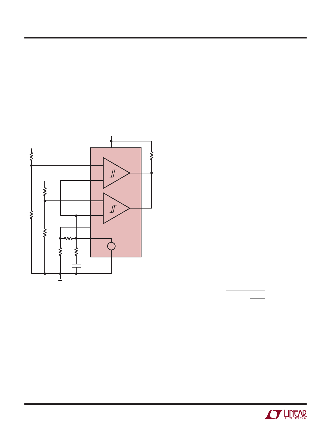
square wave applied to the V + pin. Resistors R2 and R3 set
10mV of hysteresis voltage band while R1 damps the
reference response. Note that the comparator output
doesn’t trip.
REFERENCE
OUTPUT
R1
REF
LTC144X
C1
V–
1440/1/2 F01
Figure 1. Damping the Reference Output
Comparator Outputs
The LTC1440 comparator output swings between GND
1000
and V + to assure TTL compatibility with a split supply. The
LTC1441 and LTC1442 outputs swing between V – and V +.
100
The outputs are capable of sourcing up to 40mA and
sinking up to 5mA while still maintaining microampere
10
quiescent currents. The output stage does not generate
crowbar switching currents during transitions which helps
minimize parasitic feedback through the supply pins.
1
Voltage Reference
The internal bandgap reference has a voltage of 1.182V
referenced to V –. The reference accuracy is 1.5% from
– 40°C to 85°C. It can source up to 200µA and sink up to
20µA with a 5V supply. The reference can drive a bypass
0.1
0.001
0.01
0.1
1
CAPACITOR VALUE (µF)
10
1440/1/2 F02
Figure 2. Damping Resistance vs Bypass Capacitor Value
10
144012fc
Share Link: 