AT43310 View Datasheet(PDF) - Atmel Corporation
Part Name
Description
Manufacturer
AT43310 Datasheet PDF : 25 Pages
| |||
AT43310
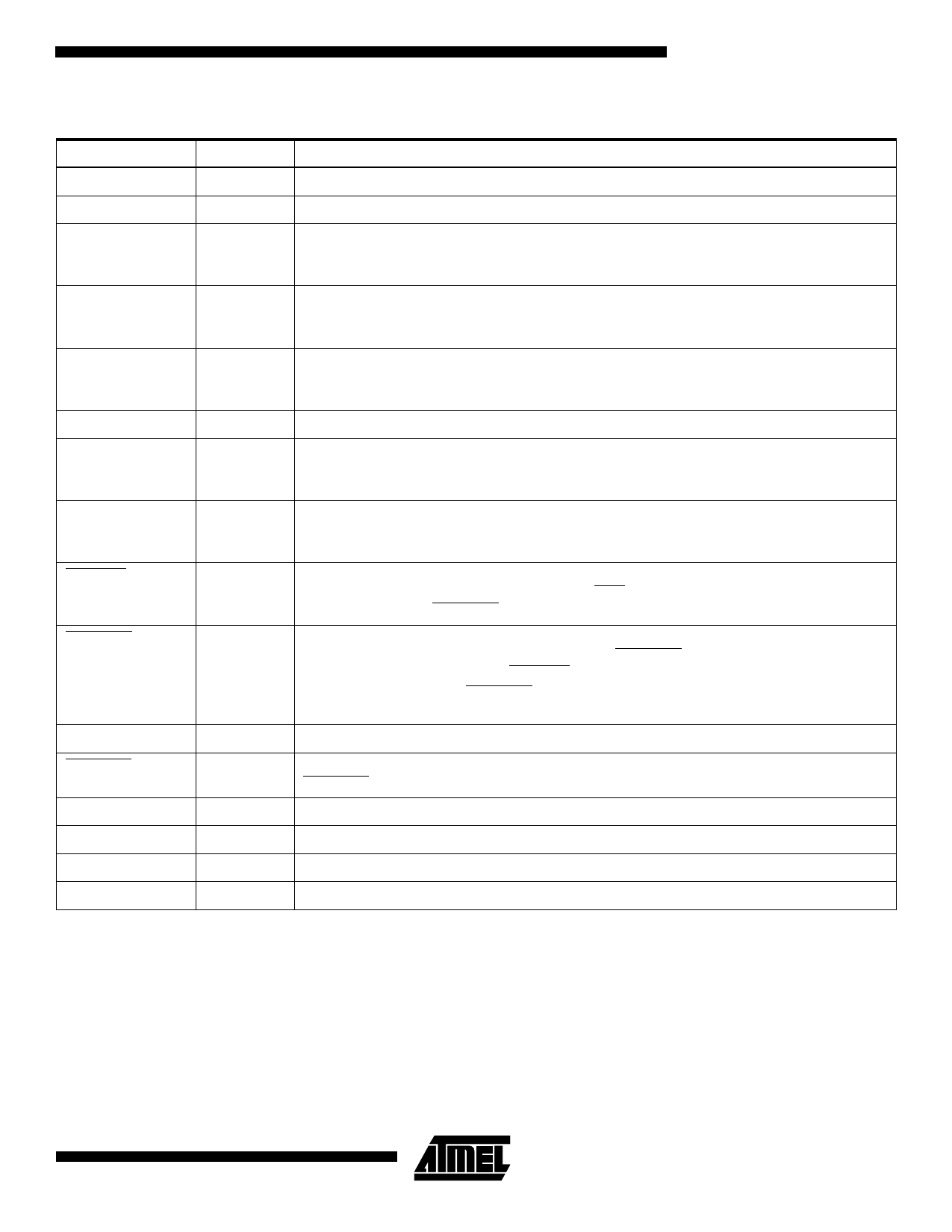
Pin Description
Pin Description
OSC1
OSC2
Pin Type
I
O
LFT
I
VREF
I
DP0
B
DM0
B
DP[1:4]
B
DM[1:4]
B
OVL[1:4]
I
PWR[1:4]
OD
Description
Oscillator Input. Input to the inverting 6 MHz oscillator amplifier.
Oscillator Output. Output of the inverting oscillator amplifier.
PLL Filter. For proper operation of the PLL, this pin should be connected through a
100 Ω resistor and 10 nF capacitor to ground (VSS) in parallel with a 2.2 nF capacitor
(see Figure 1–Power Supply Connection).
Reference Voltage. This is an input pin that should be connected to an external
voltage source. VREF is used internally as the reference voltage by the overload
protection circuit to decide whether there is a problem with a port’s power supply.
Upstream Plus USB I/O. This pin should be connected to VCC3 through an external
1.5K Ω pullup resistor. DP0 and DM0 form the full speed differential signal pin pairs
connected to the Host Controller or an upstream Hub.
Upstream Minus USB I/O
Port Plus USB I/O. These pins should be connected to VSS through external 1.5K Ω
resistors. DP[1:4] and DM[1:4] are the differential signal pin pairs to connect
downstream USB devices.
Port Minus USB I/O. These pins should be connected to VSS through external 15K Ω
resistors. DP[1:4] and DM[1:4] are the differential signal pin pairs to connect
downstream USB devices.
Port Overload. These are the input signals used to indicate to the AT43310 that there
is a power supply problem with the port. If OVL is asserted, the AT43310 will assert
the corresponding PWR[1:4] pin and report the status to the USB Host.
Power Switch. These are the output signals used to enable or disable the external
voltage regulator supplying power to the port. PWR[1:4] is de-asserted when a power
supply problem is detected at OVL[1:4].
For proper operation of PWR[1:4], an external pull-up resistor of 10K Ω to VCC5 is
required.
STAT[1:4]
VCC3
VCC5
VCCA
GND
O
Connect Status. These are output pins indicating that a port is properly connected.
STAT[1:4] is asserted when the port is enabled.
V
3.3V Power Supply, used for the USB interface
V
5V Power Supply, main power supply for the AT43310
V
5V Analog Power Supply
V
Ground
3
Share Link: 