LA7391AN View Datasheet(PDF) - SANYO -> Panasonic
Part Name
Description
Manufacturer
LA7391AN Datasheet PDF : 11 Pages
| |||
LA7391AN
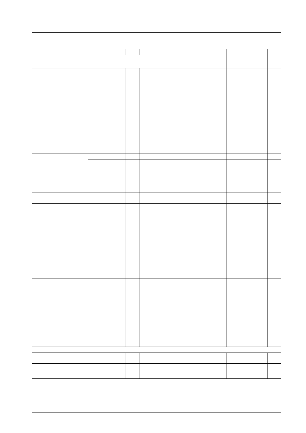
Continued from preceding page.
Parameter
FM demodulation linearity
Symbol
LDEM
Input Output
Conditions
LDEM = VDEM4V–DE(VMD6E–MV6D+EVM2DEM2)/2x 100
min typ max Unit
–3.5 0 3.5 %
Carrier leak
PB YNR characteristics
LP/EP
PB LNC characteristics
SP
Playback through gain
Nonlinear de-emphasis
characteristics
Noise canceller
characteristics
PIC-CTL center response
characteristics
PIC-CTL hard response
characteristics
PIC-CTL soft response
characteristics
Sync tip level,
pedestal level,
white level measurement
(PB)
Pseudo V insertion level
(PB)
Pseudo H insertion level
(PB)
White insertion level (PB)
Sync separation output level
Sync separation output
pulse width
Sync separation output
leading edge delay time
4.2 V regulator operation
check
[REC Mode Chroma]
REC chroma low-band
conversion output level
Burst emphasis amount
(NTSC mode)
CL
GP-YNR
GP-LNC
GPB
GNLDEEM1
GNLDEEM2
GWNC1
GWNC2
GWNC3
GPC
GPH
GPS
LVOR
∆ VDP
∆ HDP
∆WHP
VSYP
PWSYP
∆ TSYP
VREG
VOR-15
GBE
T39A
T4A
T4A
T4A
T4A
T4A
T4A
T4A
T4A
T4A
T4A
T4A
T4A
T4A
T4A
T4A
T4A
T4A
T4A
T37A
T37A
T3 VIN = 300 mVp-p, f = 4 MHz
Ratio between 4 MHz component of T3 and
SDEM
T28A VIN = white 50% + CW (15.8 mVp-p)
Ratio between 32fH component and 32.5fH
component
T28A VIN = white 50% + CW (15.8 mVp-p)
Ratio between 32fH component and 32.5fH
component
T34A Apply VIN = 0.5 Vp-p video signal to pin 4,
and determine ratio between T34A output
level and input level
T34A VIN = white 50% + CW (f = 1 MHz, 158
mVp-p)
measure input/output response, difference
with GPB
T34A f = 1 MHz, 50 mVp-p
T34A f = 1.5 MHz, 158 mVp-p
T34A f = 1.5 MHz, 50 mVp-p
T34A f = 1.5 MHz, 15.8 mVp-p
T34A f = 2 MHz, 158 mVp-p
–11
–7.0
4.0
–2.8
–5.0
–1.3
–4.5
–10.5
1.2
T34A f = 2 MHz, 158 mVp-p
7.0
T34A f = 2 MHz, 158 mVp-p
–10.0
T34 With VIN = white 100% and T34A at 1.0
Vp-p, measure electric potential for each of
the pin 34 video output sync tip, pedestal,
and white peak, and assign the measured
values to LSYN, LPED, and LWHI, respectively
T34 Measure pin 34 DC voltage when 5 V is
–80
applied to pin 33, and assign the measured
value to LVDP, and calculate the difference
with LSYN
∆ VDP = LSYN – LVDP
T34 Measure pin 34 DC voltage when 2.7 V is
–300
applied to pin 33, and assign the measured
value to LHDP, and calculate the difference
with LPED
∆HDP = LPED – LHDP
T34 Measure pin 34 DC voltage when 1.3 V is
20
applied to pin 33, and assign the measured
value to LWHP, and calculate the difference
with LWHI
∆WHP = LWHI – LWHP
T32 VIN = 0.5 Vp-p video signal, pin 32 output
4.0
pulse wave high value
T32 VIN = 0.5 Vp-p video signal, T32 output pulse 4.4
width
T32 VIN = 0.5 Vp-p video signal, measure delay 0.9
time of output SYNC versus input SYNC
T30 Measure DC level of T30 in REC mode
3.95
T15A VIN = standard color bar signal (1 Vp-p),
120
measure burst level at T15A
T15A VIN = standard color bar signal (1 Vp-p)
5.5
Ratio of burst level at T15A when S41A is off
(SP/EP) and on (LP)
–40
–9
–5.5
5.5
–1.8
–4.0
–0.8
–3.5
–9.0
1.7
8.0
–8.0
0
–200
120
4.2
4.7
1.1
4.15
160
6.0
–35 dB
–7 dB
–4.0 dB
7.0 dB
–0.8 dB
–3.0 dB
–0.3 dB
–2.5 dB
–7.5 dB
2.2 dB
10.0 dB
–7.0 dB
80 mV
–100 mV
220 mV
4.4 Vp-p
5.0 µs
1.3 µs
4.35 VDC
200 mVp-p
6.5 dB
Continued on next page.
No. 3951-4/11
Share Link: 