MSM98P05 View Datasheet(PDF) - Oki Electric Industry
Part Name
Description
Manufacturer
MSM98P05 Datasheet PDF : 14 Pages
| |||
¡ Semiconductor
MSM98P05
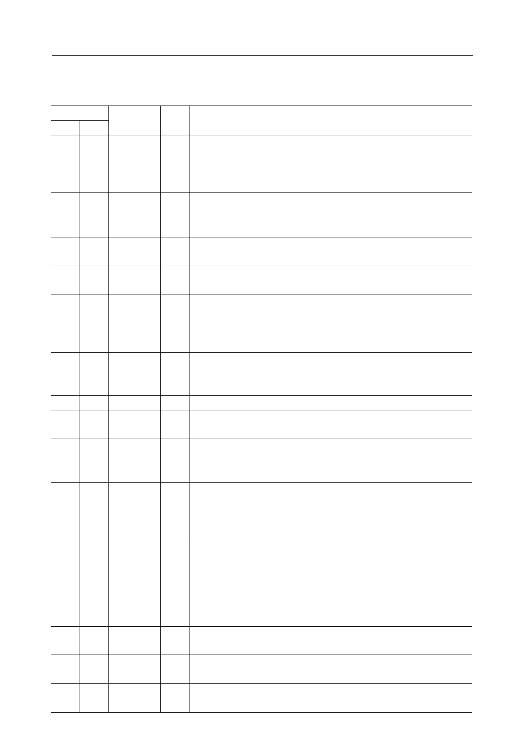
PIN DESCRIPTIONS
Pin
Symbol Type
DIP SOP
Description
The IC enters the standby state if this pin is set to "L" level. At this time,
5
17
RESET
oscillation stops and AOUT drives a current of 0mA and becomes GND level,
I
then the IC returns to the initial state. If the power cannot be applied within 1ms,
apply an "L" pulse during power-on. This pin has an internal pull-up resistor.
Signal output pin that indicates whether the register in the address controller
7 20
NAR
O to latch the 10-15 addresses (see Block Diagram) is idle. NAR at "H" level
indicates that the LATCH is empty and ST input is enabled.
6 18
XT/CR
XT/RC switching pin. Set to "H" level if ceramic oscillation is used. Set to "L"
I
level if RC oscillation is used.
15
7
CPU/STD
Microcontroller interface/stand-alone mode switching pin. Set to "H" level if
I
the IC is used in microcontroller interface mode.
Volume setting pin. If this pin is set to GND level, the maximum amplitude is
9 23
VREF
I delivered. If this pin is set to VDD level, the minimum amplitude is delivered.
This pin is internally connected to a pull-down resistor of approx. 10 kW
during IC operation.
Voice output pin.
10 24
AOUT
O The voice signals are output as current changes. A logic "L" is output from
this pin in standby state.
8 22
GND
— Ground pin.
11 1
Power supply pin. Insert a bypass capacitor of 0.1 mF or more between this
VDD
—
pin and the GND pin.
Ceramic oscillator connection pin when ceramic oscillation is selected.
12 2
OSC1
I RC connection pin when RC oscillation is selected.
Input from this pin if external clock is used.
Ceramic oscillator connection pin when ceramic oscillation is selected.
13 3
OSC2
RC connection pin when RC oscillation is selected.
O
Leave this pin open if external clock is used.
Outputs "L" level in standby state.
Leave this pin open when ceramic oscillation is used.
14 5 OSC3/TEST O RC connection pin when RC oscillation is selected.
Outputs "H" level in standby state when RC oscillation is selected.
Voice synthesis starts at fall of ST, and addresses I0 to I5 are fetched at rise
16 8
ST
I of ST. Input ST when NAR, the status signal, is at "H" level.
This pin has internal pull-up resistor.
17-19
10-15
2-4
I0 - I5
Phrase input pins corresponding to vocalized sound.
I
Power supply pin for writing to the built-in OTP. This pin should be set to "H"
1 16
VPP
—
level or be open.
20 9
PGM
Interface pin for writing to the built-in OTP. This pin should be set to "L" level
I
or be open.
10/13
Share Link: 