ADP3157 View Datasheet(PDF) - Analog Devices
Part Name
Description
Manufacturer
ADP3157 Datasheet PDF : 12 Pages
| |||
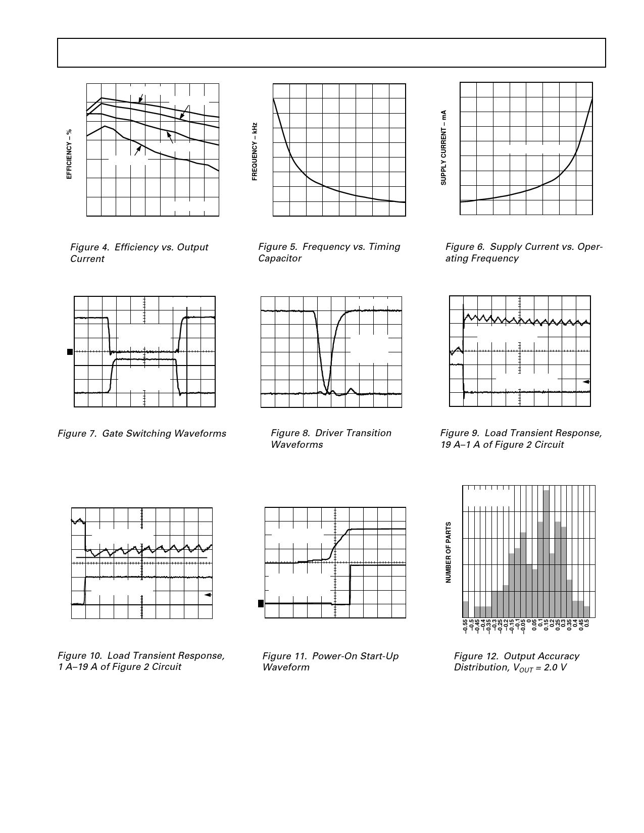
100
VOUT = 3.5V
95
VOUT = 2.8V
90
85
VOUT = 2.0V
80
VOUT = 1.3V
75
70
SEE FIGURE 2
65
1.4 2.8 4.2 5.6 7 8.4 9.8 11.2 12.6 14
OUTPUT CURRENT ŌĆō Amps
Figure 4. Efficiency vs. Output
Current
Typical Performance CharacteristicsŌĆōADP3157
450
400
350
300
250
200
150
100
50
0
50 100 200 300 400 500 600 700 800
TIMING CAPACITOR ŌĆō pF
Figure 5. Frequency vs. Timing
Capacitor
45
40
35
30
25
20
15
10
5
0
45
QGATE(TOTAL) = 100nC
58
83
134
397
OPERATING FREQUENCY ŌĆō kHz
Figure 6. Supply Current vs. Oper-
ating Frequency
SEE FIGURE 2
PRIMARY
N-DRIVE
DRIVER OUTPUT
1
SECONDARY
N-DRIVE
DRIVER OUTPUT
2
DRIVE 1 AND 2 = 5V/DIV
500ns/DIV
Figure 7. Gate Switching Waveforms
SEE FIGURE 2
VCC = +12V
VIN = +5V
IOUT = 10A
100ns/DIV
Figure 8. Driver Transition
Waveforms
OUTPUT VOLTAGE
20mV/DIV
OUTPUT CURRENT
1A TO 19A
10ŌÉ«s/DIV
Figure 10. Load Transient Response,
1 AŌĆō19 A of Figure 2 Circuit
VCC VOLTAGE
5V/DIV
3
REGULATOR
OUTPUT VOLTAGE
1V/DIV
4
10ms/DIV
Figure 11. Power-On Start-Up
Waveform
OUTPUT VOLTAGE
20mV/DIV
OUTPUT CURRENT
19A TO 1A
10ŌÉ«s/DIV
Figure 9. Load Transient Response,
19 AŌĆō1 A of Figure 2 Circuit
25
TA = +25žćC
SEE FIGURE 13
20
15
10
5
0
OUTPUT ACCURACY ŌĆō %
Figure 12. Output Accuracy
Distribution, VOUT = 2.0 V
REV. A
ŌĆō5ŌĆō
Share Link: 