AN5637 View Datasheet(PDF) - Panasonic Corporation
Part Name
Description
Manufacturer
AN5637 Datasheet PDF : 11 Pages
| |||
AN5637
ICs for TV
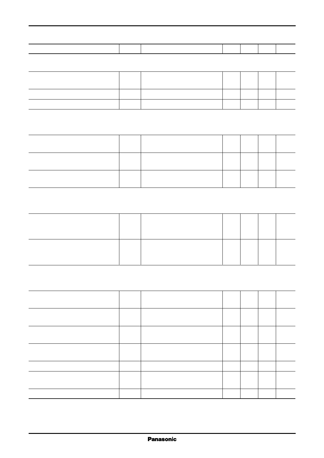
s Electrical Characteristics at VCC = 9 V, Ta = 25 °C (continued)
Parameter
Symbol
Conditions
Min Typ Max Unit
Input(Pin16)
Typical input : (Pin16) Color bar signal, (Pin15) Sand castle pulse,
(Pin1) 4.43362 MHz sine wave 350 mV[p-p], V-BLK period
Input dynamic range
Chroma signal input amplitude *1
Input impedance
Bell filter
VDR16 Composite signal input amplitude 1.0 1.5 V
range
Vch.16 Chroma signal input amplitude range 300 mV[p-p]
Z16 DC measurement
17 25 33 kΩ
Typical input : (Pin16) 4.0 MHz to 4.6 MHz sine wave 10 mV[p-p],
(Pin15) Sand castle pulse,
(Pin1) 4.43362 MHz sine wave 350 mV[p-p], V-BLK period
Bell adjusting voltage
VADB Sample hold pin voltage at bell 2.8 3.9 5
V
filter automatic adjustement
Center frequency
fOB Center frequency of bell filter
(Signal period)
4.202 4.262 4.322 MHz
Band width
B Band width of bell filter
(Signal period)
250 310 370 kHz
ACC
Typical input : (Pin16) Color bar signal (Composite) 1 V[p-p],
(Pin15) Sand castle pulse,
(Pin1) 4.43362 MHz sine wave 350 mV[p-p], V-BLK period
ACC characteristics 1
ACC1 Output change amount when
−6 0
6
%
discrimination signal changes from
150 mV[p-p] to 300 mV[p-p]
ACC characteristics 2
ACC2 Output change amount when
−6 0
6
%
discrimination signal changes from
150 mV[p-p] to 15 mV[p-p]
Demodulator/Output
Typical input : (Pin16) Color bar signal (Composite) 1 V[p-p],
(Pin15) Sand castle pulse,
(Pin1) 4.43362 MHz sine wave 350 mV[p-p], V-BLK period
PLL adjusting voltage
VADV Sample hold pin voltage at PLL 3.1 3.7 4.3 V
automatic adjustement
R−Y output amplitude
VRY Color bar (Composite) signal input 0.85 1.00 1.15 V[p-p]
(1 V[p-p])
B−Y output amplitude
VBY Color bar (Composite) signal input 1.07 1.27 1.47 V[p-p]
(1 V[p-p])
Detector output linearity
LO Color bar (Composite) signal input −6 0
6
%
(1 V[p-p])
R−Y/B−Y output ratio
Black level adjusting voltage *2
(R−Y)(B−Y) Amplitude ratio of VRY and VBY
VAD4 Pin4 voltage when difference of
B−Y black level becomes 0
1.12 1.27 1.42 Times
1.45 2.1 2.75 V
Black level error (R−Y) *2
fBER Value referred to input frequency 10 kHz
Note) *1 : Refer to "Explanations of testing method 1"
*2 : Refer to "Explanations of testing method 2"
4
Share Link: 