532BA000210BG View Datasheet(PDF) - Silicon Laboratories
Part Name
Description
Manufacturer
532BA000210BG Datasheet PDF : 33 Pages
| |||
Si532
DUAL FREQUENCY CRYSTAL OSCILLATOR (XO)
(10 MHZ TO 1.4 GHZ)
Features
Available with any-rate output
frequencies from 10 MHz to 945 MHz
and select frequencies to 1.4 GHz
Two selectable output frequencies
3rd generation DSPLL® with superior
jitter performance
3x better frequency stability than
SAW-based oscillators
Applications
Internal fixed crystal frequency
ensures high reliability and low
aging
Available CMOS, LVPECL,
LVDS, and CML outputs
3.3, 2.5, and 1.8 V supply options
Industry-standard 5 x 7 mm
package and pinout
Pb-free/RoHS-compliant
Si5602
Ordering Information:
See page 7.
SONET/SDH
Networking
SD/HD video
Description
Test and measurement
Clock and data recovery
FPGA/ASIC clock generation
The Si532 dual frequency XO utilizes Silicon Laboratories’ advanced
DSPLL® circuitry to provide a low jitter clock at high frequencies. The Si532 is
available with any-rate output frequency from 10 to 945 MHz and select
frequencies to 1400 MHz. Unlike a traditional XO where a different crystal is
required for each output frequency, the Si532 uses one fixed crystal
frequency to provide a wide range of output frequencies. This IC based
approach allows the crystal resonator to provide exceptional frequency
stability and reliability. In addition, DSPLL clock synthesis provides superior
supply noise rejection, simplifying the task of generating low jitter clocks in
noisy environments typically found in communication systems. The Si532 IC
based XO is factory configurable for a wide variety of user specifications
including frequency, supply voltage, output format, and temperature stability.
Specific configurations are factory programmed at time of shipment, thereby
eliminating long lead times associated with custom oscillators.
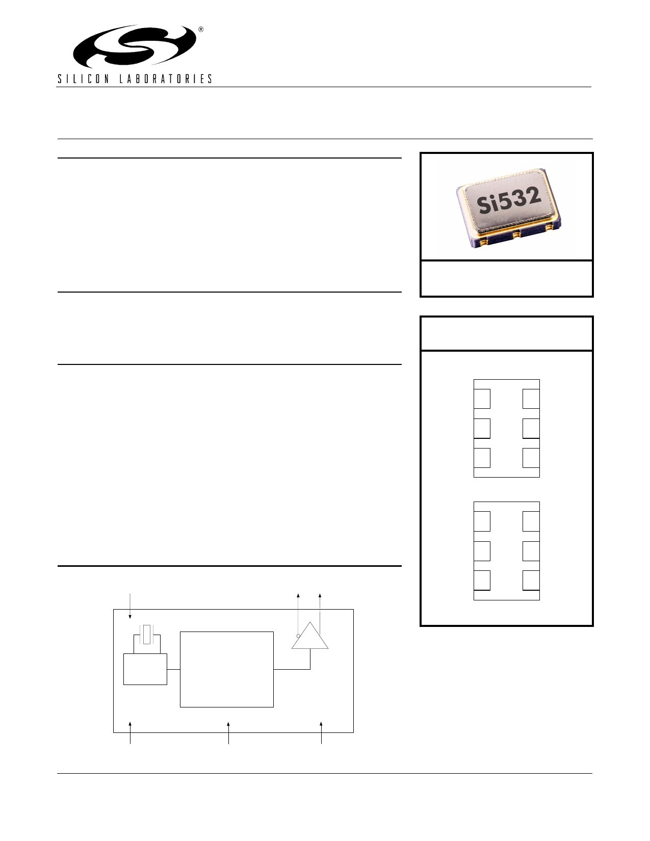
Functional Block Diagram
Pin Assignments:
See page 6.
(Top View)
FS 1
6 VDD
OE 2
5 CLK–
GND 3
4 CLK+
(LVDS/LVPECL/CML)
FS 1
OE 2
6 VDD
5 NC
GND 3
4 CLK
VDD
CLK– CLK+
(CMOS)
Fixed
Frequency
XO
Any-rate
10–1400 MHz
DSPLL®
Clock
Synthesis
FS
Rev. 1.0 7/06
OE
GND
Copyright © 2006 by Silicon Laboratories
Si532
Share Link: 