AD9601BCPZ-250 View Datasheet(PDF) - Analog Devices
Part Name
Description
Manufacturer
AD9601BCPZ-250 Datasheet PDF : 32 Pages
| |||
AD9601
THEORY OF OPERATION
The AD9601 architecture consists of a front-end sample-and-
hold amplifier (SHA) followed by a pipelined switched capacitor
ADC. The quantized outputs from each stage are combined into
a final 10-bit result in the digital correction logic. The pipelined
architecture permits the first stage to operate on a new input
sample, while the remaining stages operate on preceding
samples. Sampling occurs on the rising edge of the clock.
Each stage of the pipeline, excluding the last, consists of a low
resolution flash ADC connected to a switched capacitor DAC
and interstage residue amplifier (MDAC). The residue amplifier
magnifies the difference between the reconstructed DAC output
and the flash input for the next stage in the pipeline. One bit of
redundancy is used in each stage to facilitate digital correction
of flash errors. The last stage simply consists of a flash ADC.
The input stage contains a differential SHA that can be ac- or
dc-coupled. The output-staging block aligns the data, carries
out the error correction, and passes the data to the output
buffers. The output buffers are powered from a separate supply,
allowing adjustment of the output voltage swing. During power-
down, the output buffers go into a high impedance state.
ANALOG INPUT AND VOLTAGE REFERENCE
The analog input to the AD9601 is a differential buffer. For best
dynamic performance, the source impedances driving VIN+
and VIN− should be matched such that common-mode settling
errors are symmetrical. The analog input is optimized to provide
superior wideband performance and requires that the analog
inputs be driven differentially.
A wideband transformer, such as Mini-Circuits® ADT1-1WT,
can provide the differential analog inputs for applications that
require a single-ended-to-differential conversion. Both analog
inputs are self-biased by an on-chip resistor divider to a
nominal 1.4 V.
An internal differential voltage reference creates positive and
negative reference voltages that define the 1.25 V p-p fixed span
of the ADC core. This internal voltage reference can be adjusted
by means of SPI control. See the AD9601 Configuration Using
the SPI section for more details.
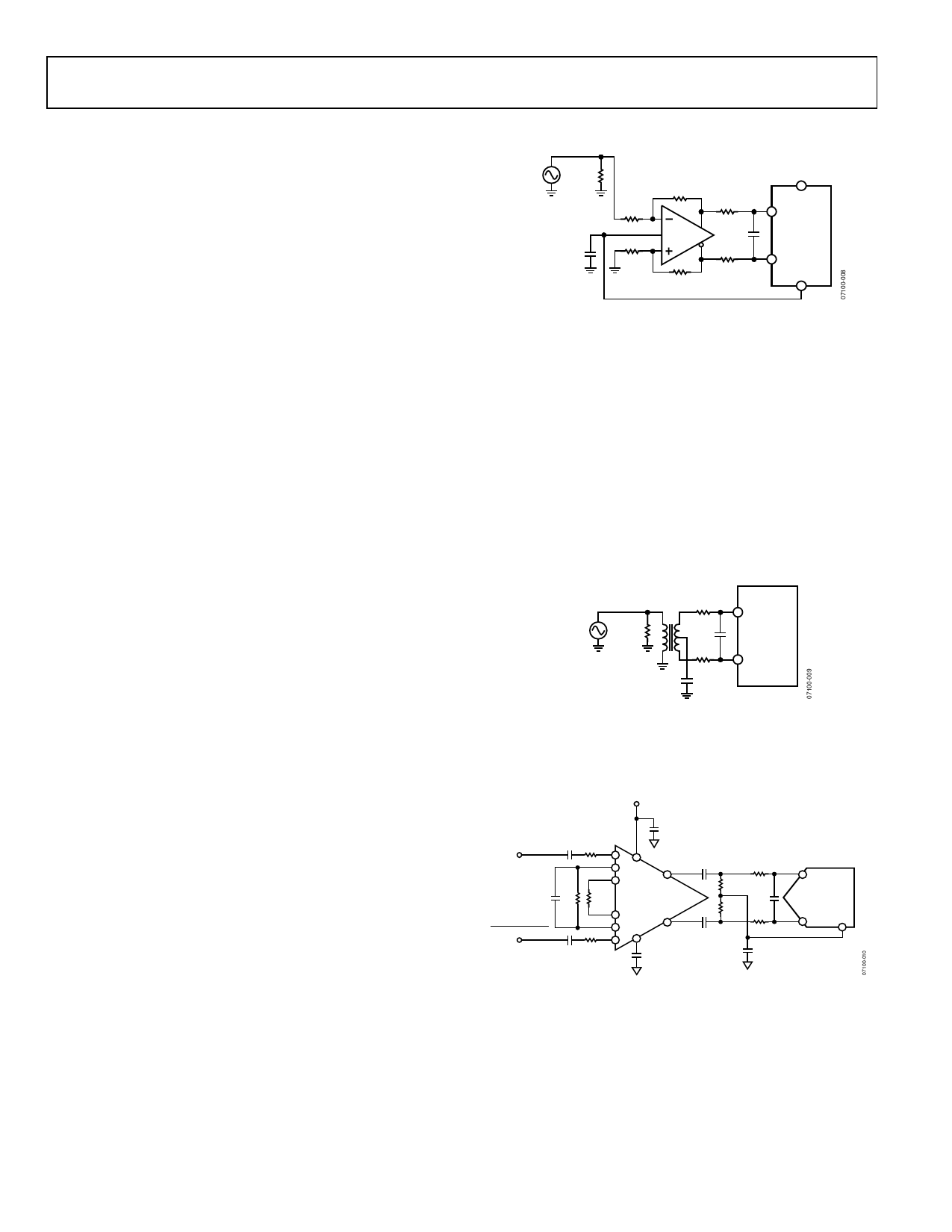
Differential Input Configurations
Optimum performance is achieved while driving the AD9601
in a differential input configuration. For baseband applications,
the AD8138 differential driver provides excellent performance
and a flexible interface to the ADC. The output common-mode
voltage of the AD8138 is easily set to AVDD/2 + 0.5 V, and the
driver can be configured in a Sallen-Key filter topology to
provide band limiting of the input signal.
1V p-p
49.9Ω
0.1µF
499Ω
523Ω
499Ω
33Ω
AD8138 20pF
33Ω
499Ω
AVDD
VIN+
AD9601
VIN–
CML
Figure 33. Differential Input Configuration Using the AD8138
At input frequencies in the second Nyquist zone and above, the
performance of most amplifiers may not be adequate to achieve
the true performance of the AD9601. This is especially true in
IF undersampling applications where frequencies in the 70 MHz
to 100 MHz range are being sampled. For these applications,
differential transformer coupling is the recommended input
configuration. The signal characteristics must be considered
when selecting a transformer. Most RF transformers saturate at
frequencies below a few millihertz, and excessive signal power
can also cause core saturation, which leads to distortion.
In any configuration, the value of the shunt capacitor, C, is
dependent on the input frequency and may need to be reduced
or removed.
1.25V p-p
15Ω
50Ω
2pF
15Ω
0.1µF
VIN+
AD9601
VIN–
Figure 34. Differential Transformer-Coupled Configuration
As an alternative to using a transformer-coupled input at
frequencies in the second Nyquist zone, the AD8352 differential
driver can be used (see Figure 35).
VCC
ANALOG INPUT
0.1µF
0Ω 16
1
2
CD
ANALOG INPUT
RD
RG
3
4
5
0.1µF 0Ω
0.1µF
8, 13
11
AD8352
10
0.1µF
R
200Ω
C
0.1µF 200Ω R
14
0.1µF
0.1µF
VIN+
AD9601
VIN– CML
Figure 35. Differential Input Configuration Using the AD8352
Rev. 0 | Page 16 of 32
Share Link: 