HM83 View Datasheet(PDF) - Unspecified
Part Name
Description
Manufacturer
HM83 Datasheet PDF : 8 Pages
| |||
H0
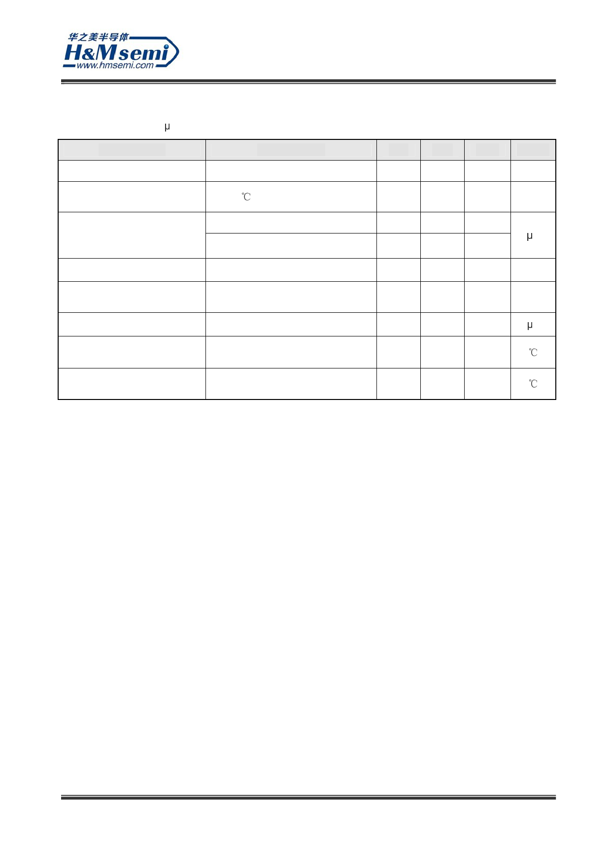
Electrical Characteristics (REG2,REG3)
VINL = 3.6V, COUT2 = 1µF, TA = 25°C, unless otherwise specified.
PARAMETER
CONDITIONS
Input Operating Range
Output Voltage Regulation
Accuracy
TA=25℃
Supply Current Per Output
Regulator Enabled
Regulator Disabled
FB2,3 Voltage
Output Current Limit
Stable COUT2,3 Range
Thermal
Temperature
Shutdown Temperature Rising
Thermal
Hysterics
Shutdown Temperature Falling
MIN TYP MAX UNITS
2
5.5
V
-1.2 VOUT2,3
+2
%
50
µA
0
1.212
V
300
mA
1
20
µF
160
℃
20
℃
Application Information
VIN (PIN1): Power Input for REG1. Bypass to GND with a high quality ceramic capacitor placed as
close as possible to the REG1.
SW (PIN2): Switching node Output for REG1. Connect this pin to the switching end of the inductor.
GND (PIN3): Power Ground, as close to the IC as possible.
VOUT2 (PIN4): Output voltage for REG2, capable of delivering up to 300mA of output current.
FB2 (PIN5): Output Feedback Sense. Receives the feedback voltage from an external resistive divider
across the output. The output voltage for REG1 is set by a resistive divider according to the following
formula: VOUT2 = 1.212V • [1 + (R3/R4)].
VINL (PIN6): Power input for REG2, REG3. Bypass to GND with a high quality ceramic capacitor placed
as close as possible to the IC.
VOUT3 (PIN7): Output voltage for REG3, capable of delivering up to 300mA of output current.
FB3 (PIN8): Output Feedback Sense. Receives the feedback voltage from an external resistive divider
across the output. The output voltage for REG3 is set by a resistive divider according to the following
4
Share Link: 