MCP120-300DI View Datasheet(PDF) - Microchip Technology
Part Name
Description
Manufacturer
MCP120-300DI Datasheet PDF : 16 Pages
| |||
MCP120/130
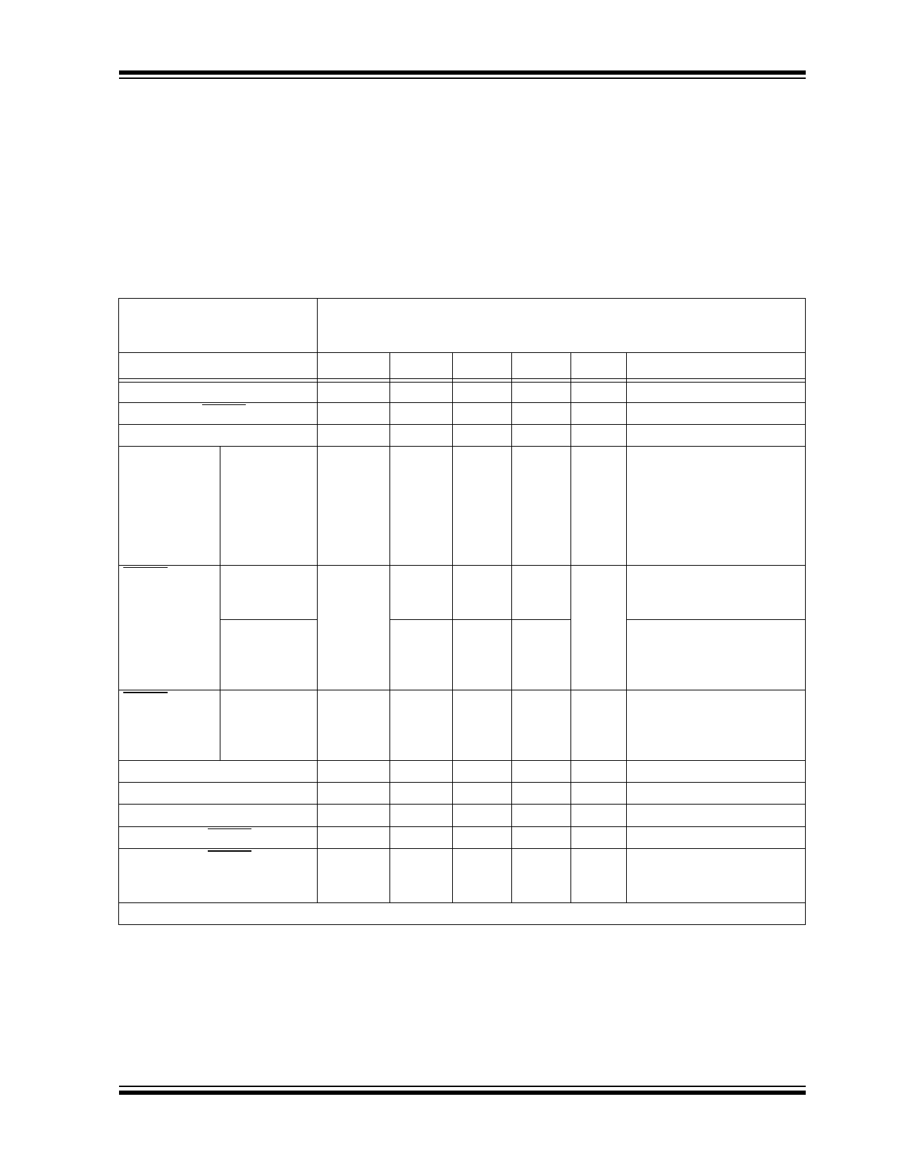
1.0 ELECTRICAL CHARACTERISTICS
1.1 Maximum Ratings*
VDD........................................................................ 7.0V
All inputs and outputs w.r.t. VSS .....-0.6V to VDD +1.0V
Storage temperature .......................... -65°C to +150°C
Ambient temp. with power applied ..... -65°C to +125°C
ESD protection on all pins ..................................... ≥ 2 kV
DC AND AC CHARACTERISTICS
*Notice: Stresses above those listed under “Maximum
Ratings” may cause permanent damage to the device.
This is a stress rating only and functional operation of
the device at those or any other conditions above those
indicated in the operational listings of this specification
is not implied. Exposure to maximum rating conditions
for extended periods may affect device reliability.
All parameters apply at the
VDD = 1.0 - 5.5V
specified temp and voltage
Industrial (I): -40°C to +85°C
ranges unless otherwise noted.
Parameter
Symbol Min.
Typ.
Operating Voltage Range
VDD Value to RESET
Operating Current
VDD Trip Point
MCP1X0-270
MCP1X0-300
MCP1X0-315
MCP1X0-450
MCP1X0-460
MCP1X0-475
MCP1X0-485
RESET Low
Level Output
Voltage
MCP1X0-270
MCP1X0-300
MCP1X0-315
MCP1X0-450
MCP1X0-460
MCP1X0-475
MCP1X0-485
RESET High
Level Output
Voltage
(MCP130 Only)
MCP130-xxx
(All VTRIP
Points)
Pull-up Resistor (MCP130 Only)
Output Leakage (MCP120 Only)
Threshold Hysteresis
VDD Detect to RESET Inactive
VDD Detect to RESET
VDD
VDDMIN
IDD
VTRIP
VOL
VOH
VHYS
tRPU
tRPD
1.0
—
1.0
—
—
45
2.55 2.625
2.85 2.925
3.0
3.075
4.25 4.375
4.35 4.475
4.50 4.625
4.60 4.725
—
—
—
—
VDD-0.7 —
—
5
—
1
—
50
150
350
—
10
Note: Typical values are for 25°C and VDD = 5.0V
Max.
5.5
—
60
2.7
3.0
3.15
4.50
4.60
4.75
4.85
0.4
0.6
—
—
—
—
700
—
Units
Test Conditions
V
V
µA VDD = 5.5V (no load)
V
V IOL = 3.2 mA,
VDD = VTRIPMIN
IOL = 8.5 mA,
VDD = VTRIPMIN
V
IOH = 50 µA,VDD > VTRIPMAX
kΩ
µA
mV
ms
µs VDD ramped from VTRIPMAX +
250 mV down to VTRIPMIN -
250 mV
2001 Microchip Technology Inc.
DS11184D-page 2
Share Link: 