TDA8932T-T View Datasheet(PDF) - NXP Semiconductors.
Part Name
Description
Manufacturer
TDA8932T-T Datasheet PDF : 45 Pages
| |||
NXP Semiconductors
TDA8932
Class-D audio amplifier
If two or more TDA8932 devices are used in the same audio application, it is
recommended to synchronize the switching frequency of all devices. This can be realized
by connecting all pins OSCIO together and configure one of the TDA8932 in the
application as clock master, while the other TDA8932 devices are configured in slave
mode.
Pin OSCIO is a 3-state input or output buffer. Pin OSCIO is configured in master mode as
oscillator output and in slave mode as oscillator input. Master mode is enabled by applying
a resistor while slave mode is entered by connecting pin OSCREF directly to pin VSSD(HW)
(without any resistor).
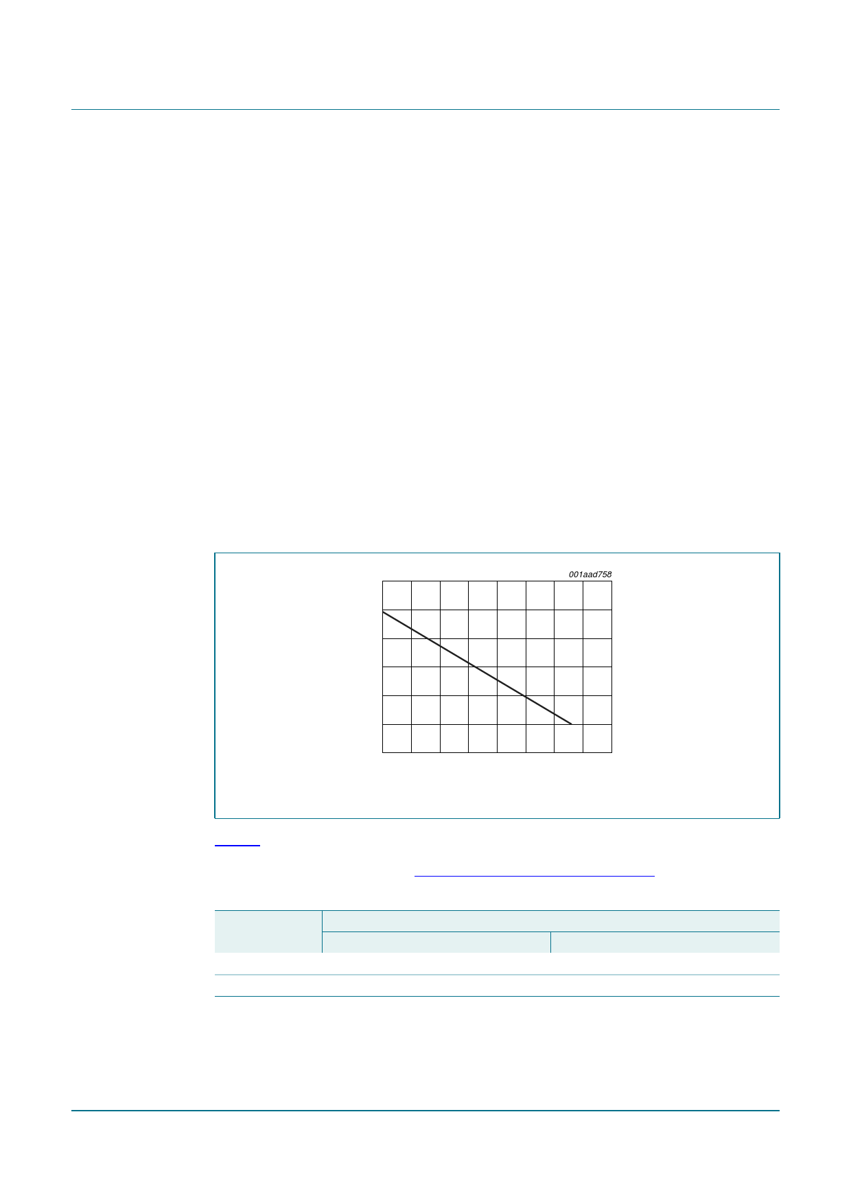
The value of the resistor also sets the frequency of the carrier which can be estimated by
the following formula:
f osc = 1----2---.-4-R--5--o---×s--c--1---0----9
(1)
Where:
fosc = oscillator frequency
Rosc = oscillator resistor (on pin OSCREF)
550
fosc
(kHz)
450
001aad758
350
250
25
30
35
40
45
Rosc (kΩ)
Fig 4. Oscillation frequency as a function of resistor Rosc
Table 5 summarizes how to configure the TDA8932 in master or slave configuration.
For device synchronization see Section 14.6 “Device synchronization”.
Table 5. Master or slave configuration
Configuration Pin
OSCREF
Master
Slave
Rosc > 25 kΩ to VSSD(HW)
Rosc = 0 Ω; shorted to VSSD(HW)
OSCIO
output
input
TDA8932_2
Preliminary data sheet
Rev. 02 — 12 December 2006
© NXP B.V. 2006. All rights reserved.
8 of 45
Share Link: 