DSP56300AD View Datasheet(PDF) - Motorola => Freescale
Part Name
Description
Manufacturer
DSP56300AD Datasheet PDF : 168 Pages
| |||
Freescale Semiconductor, Inc.
SECTION 1
SIGNAL/CONNECTION DESCRIPTIONS
SIGNAL GROUPINGS
The input and output signals of the DSP56362 are organized into functional groups, which are listed in
Table 1-1 and illustrated in Figure 1-1.
The DSP56362 is operated from a 3.3 V supply; however, some of the inputs can tolerate 5 V. A special
notice for this feature is added to the signal descriptions of those inputs.
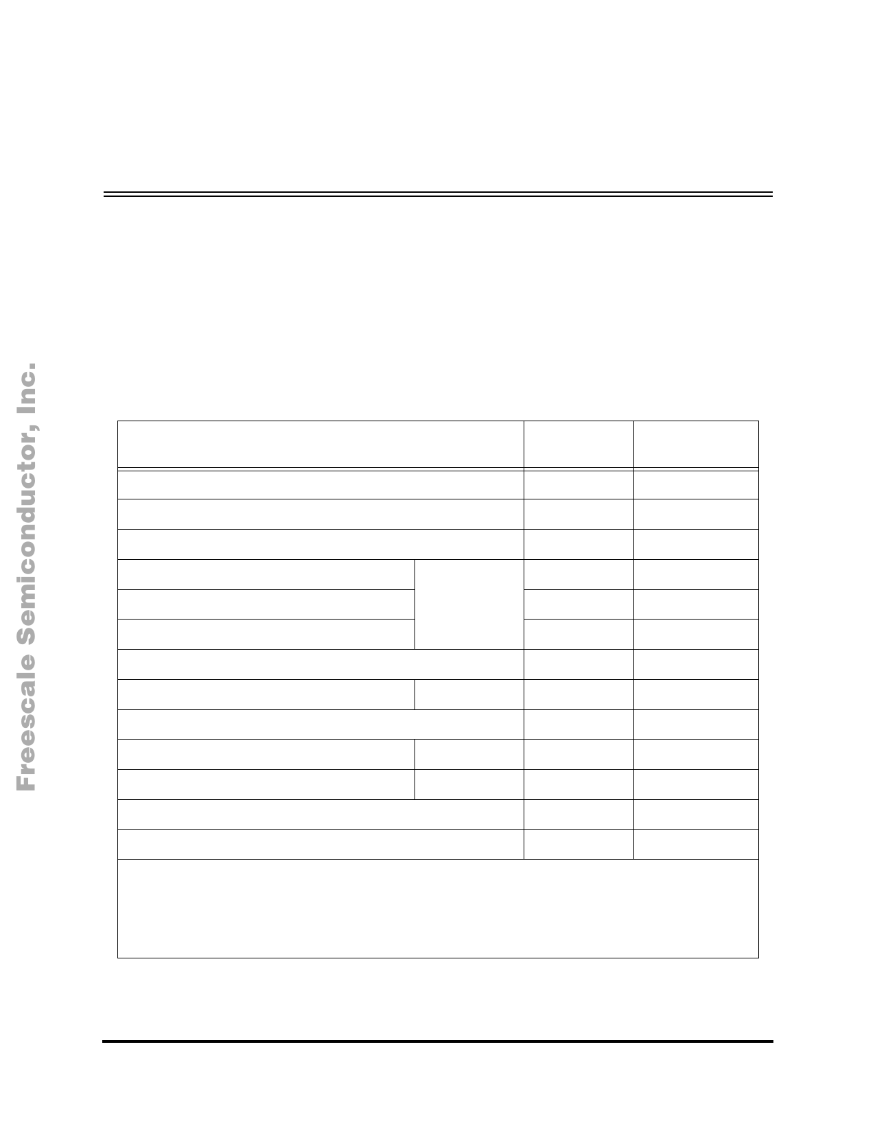
Table 1-1 DSP56362 Functional Signal Groupings
Functional Group
Number of
Signals
Detailed
Description
Power (VCC)
Ground (GND)
Clock and PLL
20
Table 1-2
19
Table 1-3
4
Table 1-4
Address bus
18
Table 1-5
Data bus
Bus control
Port A1
24
Table 1-6
11
Table 1-7
Interrupt and mode control
HDI08
5
Table 1-8
Port B2
16
Table 1-9
SHI
ESAI
Digital audio transmitter (DAX)
Port C3
Port D4
5
Table 1-10
12
Table 1-11
2
Table 1-12
Timer
1
Table 1-13
JTAG/OnCE Port
6
Table 1-14
Port A is the external memory interface port, including the external address bus, data bus, and
control signals.
Port B signals are the GPIO port signals which are multiplexed with the HDI08 signals.
Port C signals are the GPIO port signals which are multiplexed with the ESAI signals.
Port D signals are the GPIO port signals which are multiplexed with the DAX signals.
MOTOROLA
DSP56362 Advance Information
1-1
For More Information On This Product,
Go to: www.freescale.com
Share Link: 