MAX6023EBT View Datasheet(PDF) - Maxim Integrated
Part Name
Description
Manufacturer
MAX6023EBT Datasheet PDF : 13 Pages
| |||
Precision, Low-Power, Low-Dropout, UCSP
Voltage Reference
ABSOLUTE MAXIMUM RATINGS
(Voltages Referenced to GND)
IN .........................................................................-0.3V to +13.5V
OUT .............................................................-0.3V to (VIN + 0.3V)
Output Short Circuit to GND or IN (VIN < 6V) ............Continuous
Output Short Circuit to GND or IN (VIN ≥ 6V) .........................60s
Continuous Power Dissipation (TA = +70°C)
5-Bump UCSP (derate 3.4mW/°C above +70°C)........273mW
Operating Temperature Range ..........................-40°C to +85°C
Storage Temperature Range .............................-65°C to +150°C
Bump Temperature (soldering, 10s)................................+300°C
Note 1: This device is constructed using a unique set of packaging techniques that impose a limit on the thermal profile the device
can be exposed to during board-level solder attach and rework. This limit permits only the use of solder profiles recom-
mended in the industry-standard specification, JEDEC 020A, paragraph 7.6, Table 3 for IR/VPR and convection reflow.
Preheating is required. Hand or wave soldering is not allowed.
Stresses beyond those listed under “Absolute Maximum Ratings” may cause permanent damage to the device. These are stress ratings only, and functional
operation of the device at these or any other conditions beyond those indicated in the operational sections of the specifications is not implied. Exposure to
absolute maximum rating conditions for extended periods may affect device reliability.
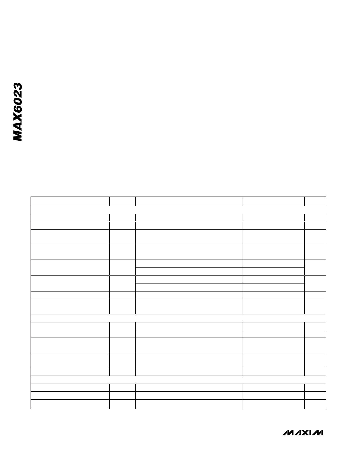
ELECTRICAL CHARACTERISTICS–MAX6023EBT12 (VOUT = 1.250V)
(VIN = +5V, IOUT = 0, TA = TMIN to TMAX, unless otherwise noted. Typical values are at TA = +25°C.) (Note 2)
PARAMETER
OUTPUT
Output Voltage
Initial Voltage Accuracy
Output Voltage Temperature
Coefficient
Line Regulation
Load Regulation
Short-Circuit Current
Temperature Hysteresis
Long-Term Stability
DYNAMIC CHARACTERISTICS
Noise Voltage
Ripple Rejection
Turn-On Settling Time
Capacitive-Load Stability Range
INPUT
Supply-Voltage Range
Supply Current
Change in Supply Current
SYMBOL
VOUT
∆VOUT/
∆VIN
∆VOUT/
∆IOUT
ISC
∆VOUT/
time
eOUT
∆VOUT/
∆IOUT
tR
COUT
VIN
IIN
∆IIN/∆VIN
CONDITIONS
TA = +25°C
TA = +25°C
(Note 3)
2.5V ≤ VIN ≤ 12.6V
0 ≤ IOUT ≤ 400µA
-400µA ≤ IOUT ≤ 0
Short to GND
Short to IN
(Note 4)
1000hr at TA = +25°C
f = 0.1Hz to 10Hz
f = 10Hz to 10kHz
VIN = +5V ±100mV, f = 120Hz
To VOUT within 0.1% of final value,
COUT = 50pF
(Note 3)
Guaranteed by line-regulation test
2.5V ≤ VIN ≤ 12.6V
MIN TYP
1.247
-0.24
1.250
10
10
0.4
0.5
4
10
90
30
25
65
86
30
0
2.5
27
0.8
MAX UNITS
1.253
V
+0.24 %
30 ppm/°C
80
µV/V
1.0
µV/µA
1.1
mA
ppm
ppm/
1000hr
µVp-p
µVRMS
dB
µs
2.2
nF
12.6
V
35
µA
2.0
µA/V
2 _______________________________________________________________________________________
Share Link: 