25VF080 View Datasheet(PDF) - Silicon Storage Technology
Part Name
Description
Manufacturer
25VF080 Datasheet PDF : 23 Pages
| |||
Advance Information
PRODUCT IDENTIFICATION
TABLE 2: PRODUCT IDENTIFICATION
Manufacturer’s ID
Device ID
SST25VF080
Address
00000H
00001H
Data
BFH
80H
T2.0 1250
MEMORY ORGANIZATION
The SST25VF080 SuperFlash memory array is organized
in 4 KByte sectors with 32 KByte overlay blocks.
8 Mbit SPI Serial Flash
SST25VF080
DEVICE OPERATION
The SST25VF080 is accessed through the SPI (Serial
Peripheral Interface) bus compatible protocol. The SPI bus
consist of four control lines; Chip Enable (CE#) is used to
select the device, and data is accessed through the Serial
Data Input (SI), Serial Data Output (SO), and Serial Clock
(SCK).
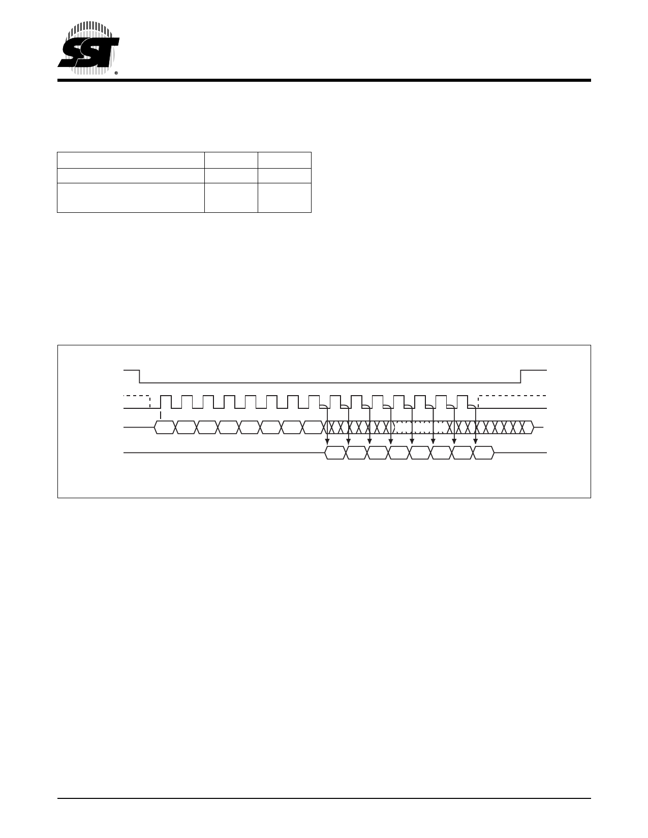
The SST25VF080 supports both Mode 0 (0,0) and Mode 3
(1,1) of SPI bus operations. The difference between the
two modes, as shown in Figure 2, is the state of the SCK
signal when the bus master is in Stand-by mode and no
data is being transferred. The SCK signal is low for Mode 0
and SCK signal is high for Mode 3. For both modes, the
Serial Data In (SI) is sampled at the rising edge of the SCK
clock signal and the Serial Data Output (SO) is driven after
the falling edge of the SCK clock signal.
CE#
MODE 3
SCK MODE 0
MODE 3
MODE 0
SI
Bit 7 Bit 6 Bit 5 Bit 4 Bit 3 Bit 2 Bit 1 Bit 0
DON'T CARE
MSB
HIGH IMPEDANCE
SO
Bit 7 Bit 6 Bit 5 Bit 4 Bit 3 Bit 2 Bit 1 Bit 0
MSB
1250 F02.0
FIGURE 2: SPI PROTOCOL
©2003 Silicon Storage Technology, Inc.
4
S71250-00-000
10/03
Share Link: 