25VF080 View Datasheet(PDF) - Silicon Storage Technology
Part Name
Description
Manufacturer
25VF080 Datasheet PDF : 23 Pages
| |||
8 Mbit SPI Serial Flash
SST25VF080
Block Protection (BP1, BP0)
The Block-Protection (BP1, BP0) bits define the size of the
memory area, as defined in Table 5, to be software pro-
tected against any memory Write (Program or Erase)
operations. The Write-Status-Register (WRSR) instruction
is used to program the BP1 and BP0 bits as long as WP#
is high or the Block-Protect-Lock (BPL) bit is 0. Chip-Erase
can only be executed if Block-Protection bits are both 0.
After power-up, BP1 and BP0 are set to 1.
Advance Information
Block Protection Lock-Down (BPL)
WP# pin driven low (VIL), enables the Block-Protection-
Lock-Down (BPL) bit. When BPL is set to 1, it prevents any
further alteration of the BPL, BP1, and BP0 bits. When the
WP# pin is driven high (VIH), the BPL bit has no effect and
its value is “Don’t Care”. After power-up, the BPL bit is
reset to 0.
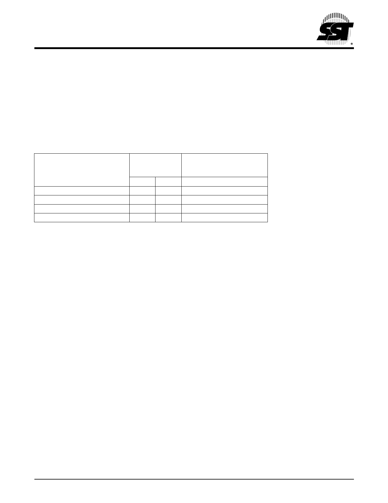
TABLE 5: SOFTWARE STATUS REGISTER BLOCK PROTECTION1
Status
Register
Bit
Protected Memory Area
Protection Level
BP1
0
0
1 (1/4 Memory Array)
0
2 (1/2 Memory Array)
1
3 (Full Memory Array)
1
1. Default at power-up for BP1 and BP0 is ‘11’.
BP0
0
1
0
1
8 Mbit
None
0C0000H-0FFFFFH
080000H-0FFFFFH
000000H-0FFFFFH
T5.0 1250
Auto Address Increment (AAI)
The Auto Address Increment Programming-Status bit pro-
vides status on whether the device is in AAI programming
mode or Byte-Program mode. The default at power up is
Byte-Program mode.
©2003 Silicon Storage Technology, Inc.
7
S71250-00-000
10/03
Share Link: 