FS6385-XX View Datasheet(PDF) - AMI Semiconductor
Part Name
Description
Manufacturer
FS6385-XX Datasheet PDF : 5 Pages
| |||
X T
March 2000
)6
7ULSOH 3// &ORFN *HQHUDWRU ,&
)25 5(9,(:
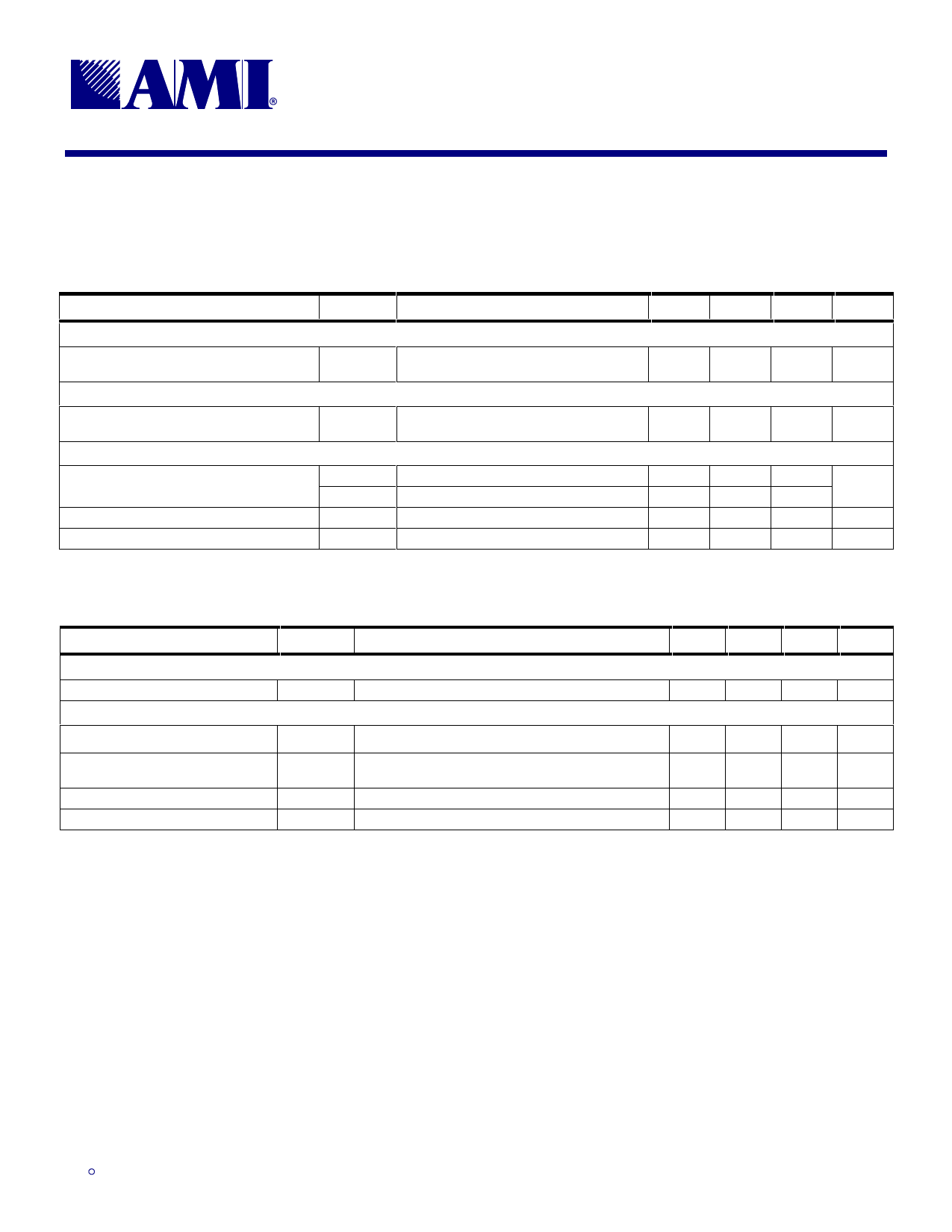
Table 5: DC Electrical Specifications
Unless otherwise stated, VDD = 3.3V ± 10%, no load on any output, and ambient temperature range TA = 0°C to 70°C. Parameters denoted with an asterisk ( * ) represent nominal characterization
data and are not production tested to any specific limits. Where given, MIN and MAX characterization data are ± 3σ from typical. Negative currents indicate current flows out of the device.
PARAMETER
SYMBOL
CONDITIONS/DESCRIPTION
MIN.
TYP. MAX. UNITS
Overall
Supply Current, Dynamic, with Loaded
Outputs
IDD
30
mA
Crystal Oscillator
Crystal Loading Capacitance
CL(xtal)
As seen by a crystal connected to XIN and
XOUT
16
pF
Clock Outputs (CLKA, CLKB, CLKC)
Output Impedance *
Short Circuit Source Current *
Short Circuit Sink Current *
zOH
VO = 0.5VDD; output driving high
zOL
VO = 0.5VDD; output driving low
IOSH
VO = 0V; shorted for 30s, max.
IOSL
VO = 3.3V; shorted for 30s, max.
45
Ω
45
-35
mA
35
mA
Table 6: AC Timing Specifications
Unless otherwise stated, VDD = 3.3V ± 10%, no load on any output, and ambient temperature range TA = 0°C to 70°C. Parameters denoted with an asterisk ( * ) represent nominal characterization
data and are not production tested to any specific limits. Where given, MIN and MAX characterization data are ± 3σ from typical.
PARAMETER
SYMBOL
CONDITIONS/DESCRIPTION
MIN. TYP. MAX. UNITS
Overall
Synthesis Error
(unless otherwise noted in Frequency Table)
0
ppm
Clock Outputs (CLKA, CLKB, CLKC)
Duty Cycle *
Jitter, Period (peak-peak) *
Ratio of high pulse width (as measured from rising edge to next falling
edge at VDD/2) to one clock period
45
55
%
tj(∆P)
From rising edge to next rising edge at VDD/2, CL =
10pF
300
ps
Rise Time *
Fall Time *
tr
VDD = 3.3V; VO = 0.3V to 3.0V; CL = 10pF
tf
VDD = 3.3V; VO = 3.0V to 0.3V; CL = 10pF
3
ns
2.5
ns
3
,62
3.24.00
Share Link: 