GL911TX View Datasheet(PDF) - Genesys Logic
Part Name
Description
Manufacturer
GL911TX Datasheet PDF : 10 Pages
| |||
GL911Tx 1.1
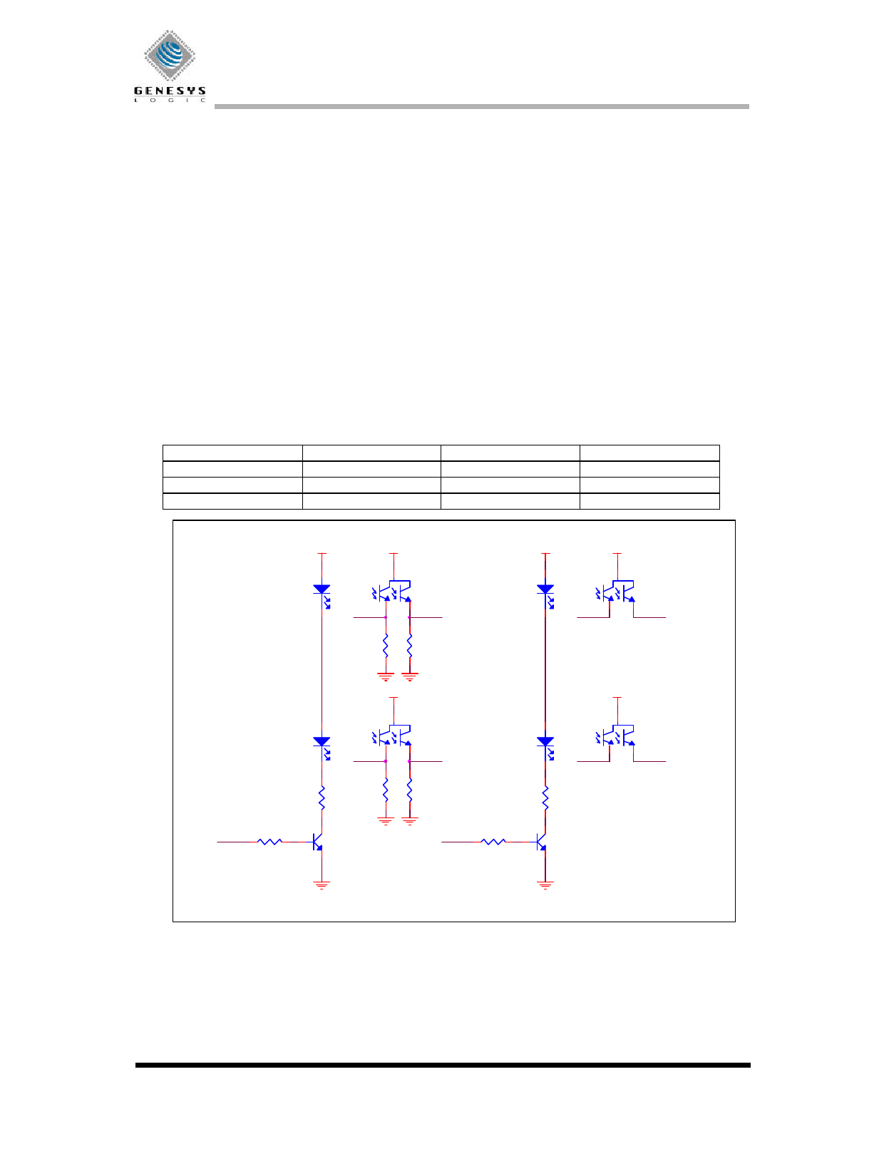
3.5 X, Y, Z, W photo sensor
(a) The X1, X2, Y1, Y2, Z1, Z2, W1, W2 are connected to PIR collector pins respectively. In order to
reduce the pin count, X/Z axis and Y/W axis are shared with the same input pins. X,Y axis’s IR
LED is controlled by XYEN pin and Z,W axis’s IR LED is controlled by ZWEN pin. Each IR
control pin is turned on periodically from 20us/per 208us (Full Speed) , 20us/per 1040us (standby
mode) and 20us/per 10ms (Sleep mode) for power saving.
(b) The photo sensor pin threshold voltage is around 0.8 Volt. It is necessary to adjust the current limit
resistor and photo sensor’s emitter resistors for different photo sensor and roller wheel mechanical
parts.
Mode
Full Speed
Standby
Sleep
Table 3-1: Period of Photo sensor active time
XYEN/ZWEN flush time
20ìs
20ìs
20ìs
Period
208ìs
1040ìs
10.40ms
State Change time
Instant
12ms
6sec
V3V
V3V
(X LED)
D4
LED
X1/Z1
Q1
PIR
X2/Z2
R2
R3
4.7K
4.7K
V3V
V3V
(Z LED)
D5
LED
X1/Z1
Q2
PIR
X2/Z2
V3V
V3V
(Y LED)
R4
180
XYEN
Q5
R10 2N3904
10K
D8
LED
Y1/W1
R12
4.7K
Q3
PIR
Y2/W2
(W LED)
R13
R5
4.7K
180
R11
ZWEN
Q6
2N3904
10K
D9
LED
Y1/W1
( Min. 208us 轉態 )
Q4
PIR
Y2/W2
Figure 3-2:GL911Tx Photo Sensor circuit example
©2000-2001 Genesys Logic Inc.—All rights reserved
-5
Share Link: 