GL650USB View Datasheet(PDF) - Genesys Logic
Part Name
Description
Manufacturer
GL650USB Datasheet PDF : 16 Pages
| |||
GL650USB 4 PORT USB HUB CONTROLLER
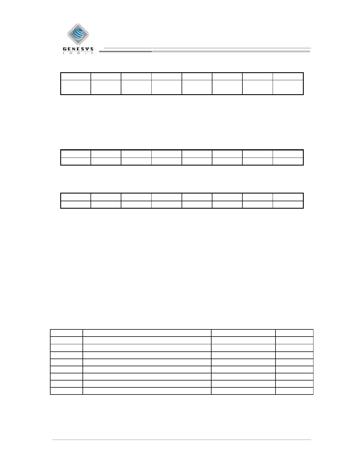
GPIOD
(offset 0F, default = 0Fh)
R/W
R/W
R/W
R/W
R/W
R/W
R/W
GPIO3D/ GPIO2D/ GPIO1D/ GPIO0D/
LED4# LED3# LED2# LED1#
General purpose I/O pin status –
If GPIOXOE = 1 (X: 0 ~ 3), GPIOX is driven with the level of internal GPIOXD latch, which
is the same as corresponding GPIOXD bit. If GPIOXOE = 0, GPIOXD reflects the level of
GPIOX pin, which may be different from internal GPIOXD latch. The value written to GPIOD
will be stored in an internal latch, no matter what direction the GPIOX pins are in. Bits 3 to 0
have been pre-assigned specific functions for LED indicators. (active low).
REV
R/O
REV7
( offset 10, default = current revision )
R/O
R/O
R/O
R/O
R/O
R/O
REV6
REV5
REV4
REV3
REV2
REV1
This register returns current silicon revision number of the HUB.
Current revision is 8’h11. (Revision 1.1)
R/O
REV0
DEVSTUS
( offset 11, default = 00h )
R/W
R/W
R/W
R/W
R/W
R/W
R/W
R/W
HCONFIG DEVADR6 DEVADR5 DEVADR4 DEVADR3 DEVADR2 DEVADR1 DEVADR0
USB device status registers. Procedure to set the device address:
1. After USB reset, the device responds to default address 0, and hub configuration = 0.
2. USB host controller issues SET_ADDRESS request to the device. (INTRB asserted)
3. Micro-controller recognizes the request, then set DEVADR register with appropriate value.
4. Micro-controller prepares the status stage of SET_ADDRESS request by programming
TXCTL0 register.
5. When the hub configuration value is not equal zero, HCONFIG is set to one.
USB reset will clear this register.
6 MAXIMUM RATINGS
Maximum ratings are the extreme limits to which the GL650USB/GL650USB-A can be exposed without
permanently damaging it. The GL650USB/GL650USB-A contain circuitry to protect the inputs against
damage from high static voltages; however, do not apply voltages higher than those shown in the table.
Keep VIN and VOUT within the range GND ≤ (VIN or VOUT) ≤ VCC. Connect unused inputs to the appropriate
voltage level, either GND or VDD.
Symbol
TSTG
TOP
VCC
VIN
I
IMGND
IMVCC
VESD
Characteristic
Storage temperature
Operating temperature
Supply voltage
DC input voltage
Maximum current per pin excluding VDD and VSS
Maximum current out of GND
Maximum current out of VCC
Static discharge voltage
Value
-55 to +150
0 to +70
-0.5 to +7.0
-0.5 to +VDD + 0.5
25
100
100
>4000
Unit
°C
°C
V
V
mA
mA
mA
V
11
08/18/00
Revision 1.2
Share Link: 