SSD1814 View Datasheet(PDF) - Solomon Systech
Part Name
Description
Manufacturer
SSD1814 Datasheet PDF : 28 Pages
| |||
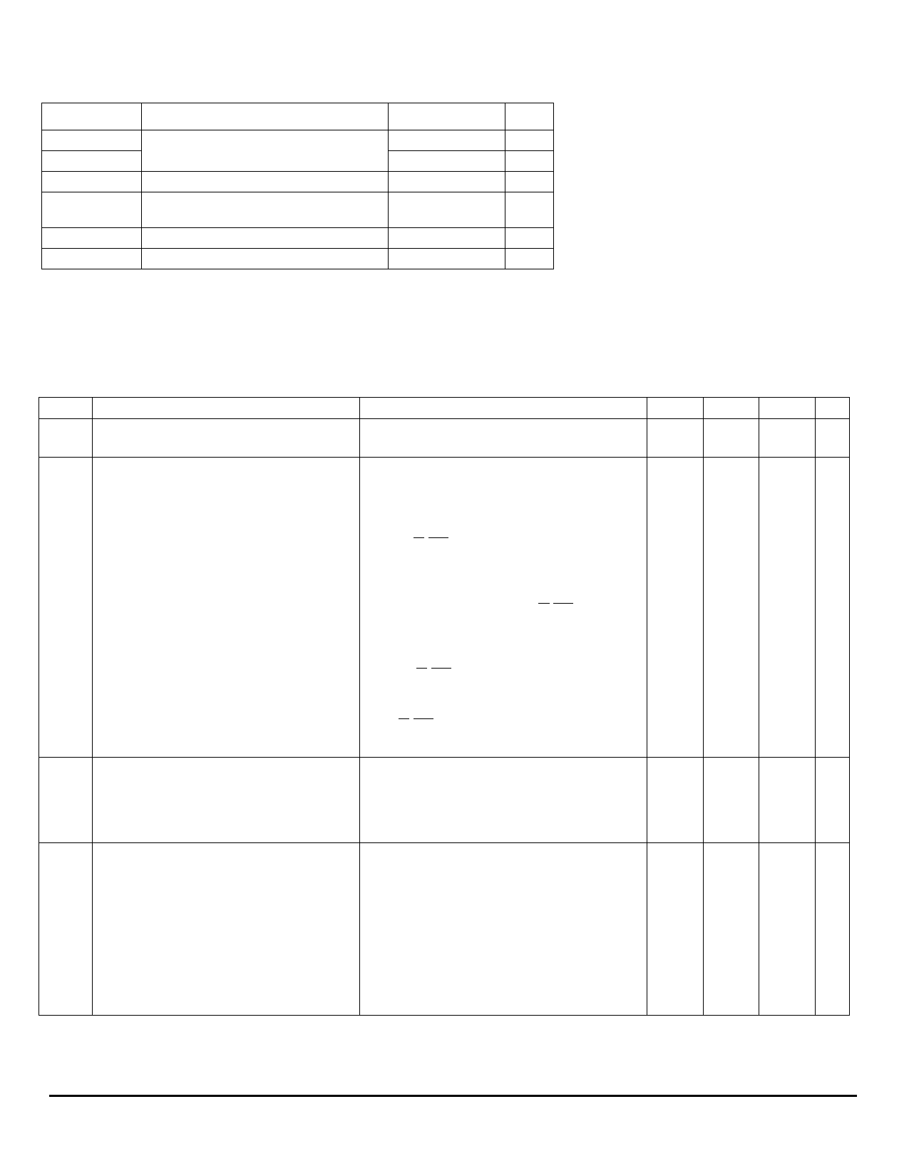
MAXIMUM RATINGS* (Voltages Referenced to VSS, TA=25°C)
Symbol
Parameter
Value
Unit
VDD
Supply Voltage
-0.3 to +4.0
V
VEE
-4.0 to -12.0
V
Vin
Input Voltage
VSS-0.3 to VDD+0.3
V
I
Current Drain Per Pin Excluding VDD and
25
mA
VSS
TA
Operating Temperature
-30 to +85
°C
Tstg
Storage Temperature Range
-65 to +150
°C
* Maximum Ratings are those values beyond which damage to the device may occur. Functional
operation should be restricted to the limits in the Electrical Characteristics tables or Pin Descrip-
tion section.
This device contains circuitry to protect the inputs
against damage due to high static voltages or elec-
tric fields; however, it is advised that normal precau-
tions to be taken to avoid application of any voltage
higher than maximum rated voltages to this high
impedance circuit. For proper operation it is recom-
mended that Vin and Vout be constrained to the
range VSS < or = (Vin or Vout) < or = VDD. Reliability
of operation is enhanced if unused input are con-
nected to an appropriate logic voltage level (e.g.,
either VSS or VDD). Unused outputs must be left
open. This device may be light sensitive. Caution
should be taken to avoid exposure of this device to
any light source during normal operation. This
device is not radiation protected.
ELECTRICAL CHARACTERISTICS (Voltage Referenced to VSS, VDD=1.8 to 3.5V, TA=25°C; unless otherwise specified.)
Symbol
Parameter
Test Condition
Min
Typ
Max Unit
VDD Logic Circuit Supply Voltage Range
Recommend Operating Voltage
Voltage Generator Circuit Supply Voltage Range Possible Operating Voltage
2.4
2.7
3.5
V
1.8
-
3.5
IAC Access Mode Supply Current Drain (VDD Pins) VDD = 2.7V, Voltage Generator On, 4X Converter
-
Enabled, Write accessing, Tcyc =3.3MHz, Osc.
Freq.=31kHz, Display On.
300
TBD µA
IDP1 Display Mode Supply Current Drain (VDD Pins) VDD = 2.7V, VEE = -8.1V, Voltage Generator Dis-
-
abled, R/W(WR) Halt, Osc. Freq. = 31kHz, Display
On, VL6 - VDD = -8.1V.
IDP2 Display Mode Supply Current Drain (VDD Pins) VDD = 2.7V, VEE = -8.1V, Voltage Generator On, 4x
-
DC-DC Converter Enabled, R/W(WR) Halt, Osc.
Freq. = 31kHz, Display On, VL6 - VDD = -8.1V.
ISB Standby Mode Supply Current Drain (VDD Pins) VDD=2.7V, LCD Driving Waveform Off, Osc. Freq. =
-
31kHz, R/W(WR) halt.
120
TBD µA
150
TBD µA
3.5
10
µA
ISLEEP Sleep Mode Supply Current Drain (VDD Pins)
VDD = 2.7V, LCD Driving Waveform Off, Oscillator
-
0.2
5
µA
Off, R/W(WR) halt.
VEE LCD Driving Voltage Generator Output
(VEE Pin)
VLCD
VOH1
LCD Driving Voltage Input (VEE Pin)
Output High Voltage
(D0-D7)
VOL1 Output Low Voltage
(D0-D7)
VL6 LCD Driving Voltage Source (VL6 Pin)
VL6 LCD Driving Voltage Source (VL6 Pin)
Display On, Voltage Generator Enabled,
DC/DC Converter Enabled, Osc. Freq.=31KHz,
Regulator Enabled, Divider Enabled.
Voltage Generator Disabled.
Iout=100µA
-12.0
-
-12.0
-
0.9*VDD
-
-1.8
V
-1.8
V
VDD
V
Iout=100µA
0
-
0.1*VDD V
Regulator Enabled (VL6 voltage depends on Int/Ext VEE-0.5
-
Contrast Control)
VDD
V
Regulator Disable
-
Floating
-
V
SSD1814 REV 0.3
8
12/99
SOLOMON
Share Link: 