SSD1809T View Datasheet(PDF) - Solomon Systech
Part Name
Description
Manufacturer
SSD1809T Datasheet PDF : 27 Pages
| |||
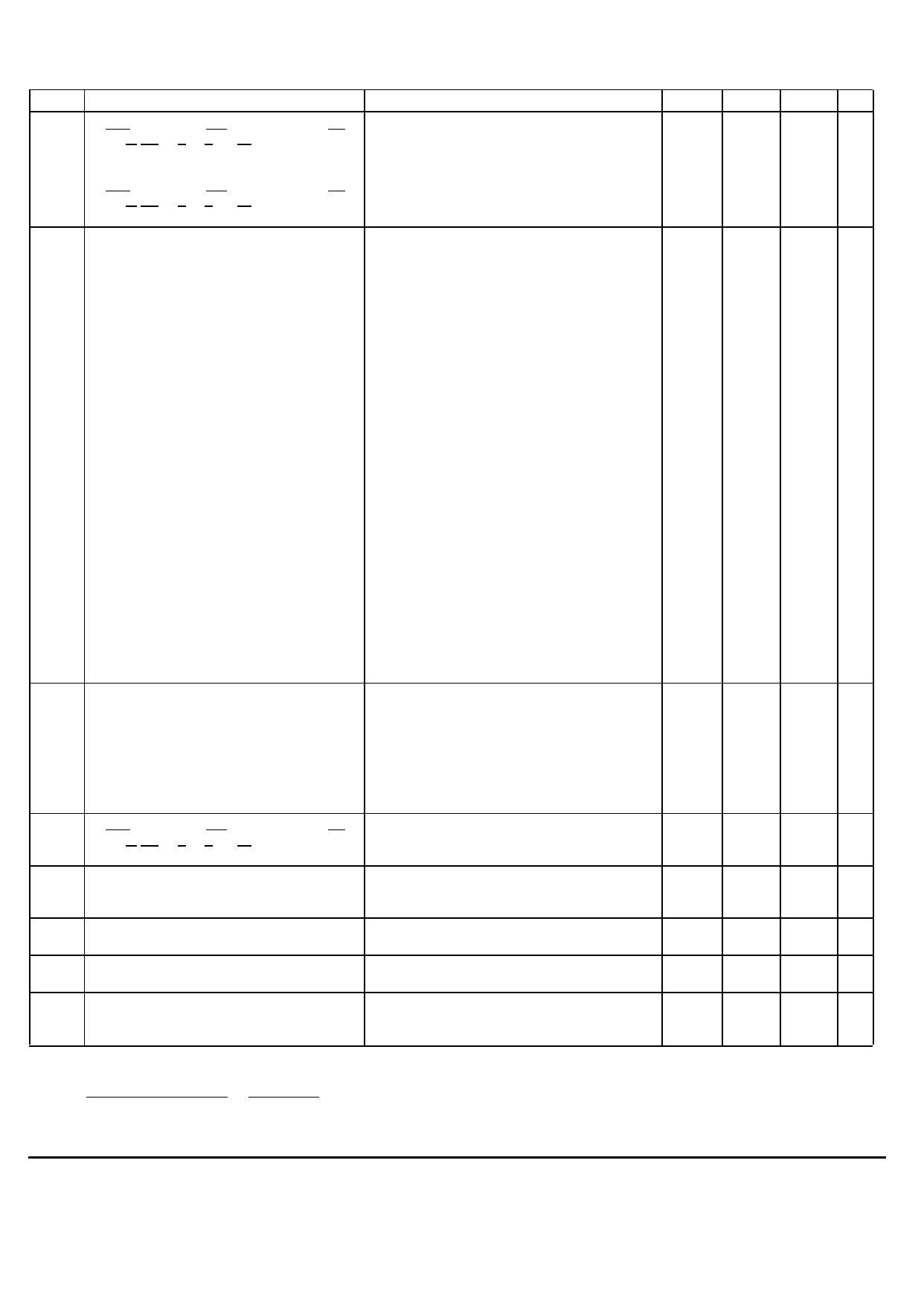
ELECTRICAL CHARACTERISTICS (Voltage Referenced to VSS, VDD=2.2 to 3.5V, TA=25°C; unless otherwise specified.)
Symbol
Parameter
Test Condition
Min
Typ
Max Unit
V IH1
VIL1
Input high voltage
(RES, OSC2, CLK/WR/SCK,SDA/D 0-D7, CE ,
R/W/RD, D/ C, P/S, 68/80, OSC1)
Input Low voltage
(RES, OSC2, CLK/WR/SCK,SDA/D 0-D7, CE ,
R/W/RD, D/ C, P/S, 68/80, OSC1)
0.8*VDD
-
VDD
V
0
-
0.2*VDD V
VLL6
VLL5
VLL4
VLL3
VLL2
LCD Display Voltage Output
(VLL6, VLL5, VLL4, VLL3, VLL2 Pins)
Voltage Divider Enabled, 1:5 bias ratio
-
VR
-
V
-
4/5*VR
-
V
-
3/5*VR
-
V
-
2/5*VR
-
V
-
1/5*VR
-
V
VLL6
VLL5
VLL4
VLL3
VLL2
LCD Display Voltage Output
(VLL6, VLL5, VLL4, VLL3, VLL2 Pins)
Voltage Divider Enabled, 1:7 bias ratio
-
VR
-
V
-
6/7*VR
-
V
-
5/7*VR
-
V
-
2/7*VR
-
V
-
1/7*VR
-
V
VLL6
VLL5
VLL4
VLL3
VLL2
LCD Display Voltage Input
(VLL6, VLL5, VLL4, VLL3, VLL2 Pins)
Voltage Divider Enabled, 1:8 bias ratio
-
VR
-
V
-
7/8*VR
-
V
-
6/8*VR
-
V
-
2/8*VR
-
V
-
1/8*VR
-
V
VLL6
VLL5
VLL4
VLL3
VLL2
LCD Display Voltage Input
(VLL6, VLL5, VLL4, VLL3, VLL2 Pins)
Voltage Divider Enabled, 1:9 bias ratio
-
VR
-
V
-
8/9*VR
-
V
-
7/9*VR
-
V
-
2/9*VR
-
V
-
1/9*VR
-
V
VLL6
VLL5
VLL4
VLL3
VLL2
IO H
LCD Display Voltage Input
(VLL6, VLL5, VLL4, VLL3, VLL2 Pins)
Output High Current Source
(SDA/D 0-D7, OSC2)
External Voltage Generator, Voltage Divider Disable
7
0
0
0
0
Vout =VDD -0.4V
50
-
VCC
V
-
VLL6
V
-
VLL5
V
-
VLL4
V
-
VLL3
V
-
-
µA
IOL Output Low Current Drain
(SDA/D 0-D7, OSC2)
Vout =0.4V
-
-
-50
µA
IO Z
IIL /IIH
Output Tri-state Current Drain Source
(SDA/D 0-D7, OSC2)
Input Current
(RES, OSC2, CLK/WR/SCK,SDA/D 0-D7, CE ,
R/W/RD, D/ C, P/S, 68/80, OSC1)
-1
-
1
µA
-1
-
1
µA
Ron Channel resistance between LCD driving signal During Display on, 0.1V apply between two termi-
-
pins (SEG and COM) and driving voltage input nals, V CC within operating voltage range
pins (V LL2 to VLL6)
VSB Memory Retention Voltage (DV DD)
Standby mode, retain all internal configuration and
2
RAM data
-
10
kΩ
-
-
V
CIN Input Capacitance
(OSC1, OSC2, all logic pins)
-
5
7.5
pF
PTC0
PTC3
Temperature Coefficient Compensation*
Flat Temperature Coefficient
Temperature Coefficient 3*
TC1=0, TC2=0, Voltage Regulator Disabled
TC1=1, TC2=1, Voltage Regulator Enabled
-
0.0
-
%
-
-0.35
-
%
*The formula for the temperature coefficient (TC) is:
TC(%)=
VR at 50°C - VR at 0°C
50°C - 0°C
1
X VR at 25°C
X 100%
SSD1809
6
REV1.3
03/02
SOLOMON
Share Link: 