VV0670P001 View Datasheet(PDF) - Vision
Part Name
Description
Manufacturer
VV0670P001 Datasheet PDF : 36 Pages
| |||
Colour Processor Interface ASIC
Camera exposure and gain values are programmed via this interface.
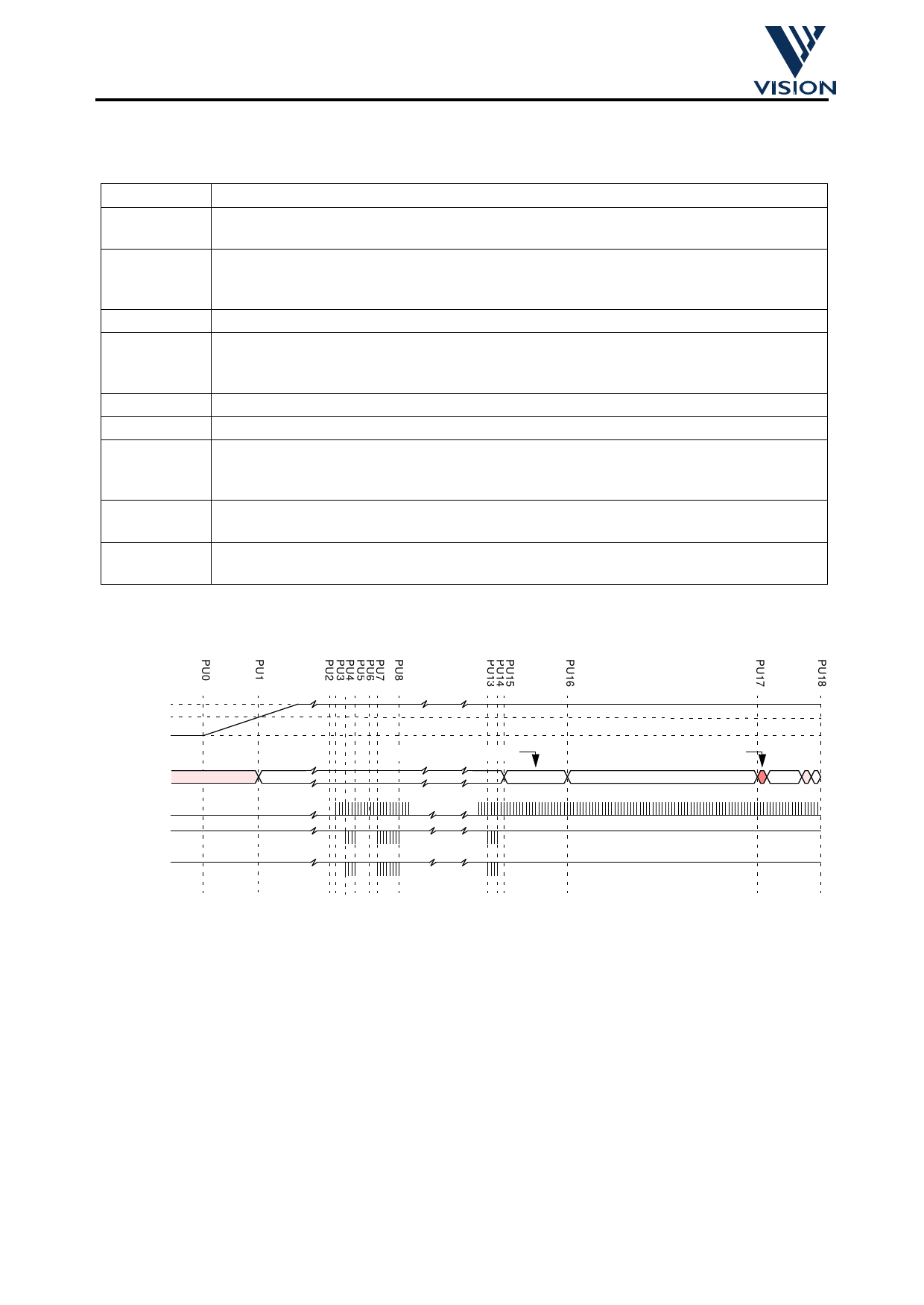
The following table and diagram illustrate the camera power up sequence.
PU0
PU1
PU2
PU3
PU4-PU5
PU6
PU7-PU8
PU13-PU4
PU15-PU16
PU17-PU18
System Power Up
Sensor Internal-on Reset Triggers, the sensor enters low power mode and
SDATA[3:0] is set to FH.
CPiA internally releases video processing modules from reset. NOTE - this event is
under the control of the Control Processor, and does not occur until the host has
requested video from the camera.
CPiA enables the sensor clock, SCLK.
At least 16 SCLK clock periods after SCLK has been enabled CPiA sends a “Soft-
Reset” command to the sensor via the serial interface. This ensures that if a sensor
is present then it is in low-power mode.
On detecting 32 consecutive FH values on SDATA [3:0], CPiA detects the camera
If present, CPiA uploads the sensor defect map from camera head E2PROM.
At least 16 SCLK clock periods after SCLK has been enabled, CPiA sends an “Exit
Low-Power Mode” command to the sensor via the serial interface. This initiates the
sensors 4 frame start sequence.
One frame of alternating 9H & 6H data on SDATA[3:0] for the CPiA to determine the
best sampling phase for the nibble data SDATA[3:0].
4 Frames after the “Exit Low-Power Mode” serial comms, the sensor starts to output valid
video data.
Regulated
Sensor
Power
SDATA[3:0]
SCLK
SSDA
SSCL
One frame of 9H & 6H data.
FH
9H,6H,9H,6H...
5V
2.8V
0V
Start of Frame Line for
the 1st frame of valid
FH
Camera Head Interface Behaviour up to and including first valid video data
V:\apps\cpia\docs\cpia datasheet\cpia_datasheet4.fm
02/07/98
9
Commercial In Confidence
Share Link: 