MC33390D/DR2 View Datasheet(PDF) - Motorola => Freescale
Part Name
Description
Manufacturer
MC33390D/DR2 Datasheet PDF : 16 Pages
| |||
Freescale Semiconductor, Inc.
SYSTEM/APPLICATION INFORMATION
INTRODUCTION
The 33390 is a serial transceiver device designed to meet
the SAE Standard J-1850 Class B performance for bi-
directional half-duplex communication. The device is packaged
in an economical surface-mount SOIC plastic package. An
internal block diagram of the device is shown in Figure 1.
The 33390 derives its robustness to temperature and voltage
extremes from being built on a SMARTMOS process,
incorporating CMOS logic, bipolar/MOS analog circuitry, and
DMOS power FETs. Though the 33390 was principally
designed for automotive applications requiring SAE J-1850
Class B standards, it is suited for other serial communication
applications. It is parametrically specified over an ambient
temperature range of -40°C ≤ TA ≤ 125°C and 7.0 V ≤ VBAT ≤
16 V supply. The economical 8-pin SOICN surface mount
plastic package makes the device a cost-effective solution.
FUNCTIONAL DESCRIPTION
Input Power (VBAT Pin)
This is the only required input power source necessary to
operate the 33390. The internal voltage reference of the 33390
will remain fully operational with a minimum of 9.0 V on this pin.
Bus transmissions can continue with battery voltages down to
5.0 V. The bus output voltage will follow the battery voltage
down and, in doing so, track approximately 1.6 V below the
battery voltage. The device will continue to receive and transmit
bus data to the microcontroller with battery voltages as low as
4.25 V. The pin can withstand voltages from -0.3 V to 40 V. If
reverse battery protection is required, an appropriate diode
must be placed in series with this pin to protect the IC.
Sleep Input (SLEEP Pin)
This input is used to enable and disable the Class B
transmitter. The Class B receiver is always enabled so long as
adequate VBAT pin voltage is applied. When the SLEEP pin
voltage is 5.0 V, the Class B transmitter is enabled. If this input
is 0 V, the Class B transmitter will be disabled and less than
65 µA of current will be drawn by the VBAT pin. The pin also
provides a 5.0 V reference, internal to the device, used to
establish the Rx output level and slew rate times.
Class B Functional Description
The transmitter provides an analog waveshaped 0 V to 7.0 V
waveform on the BUS output. It also receives waveforms and
transmits a digital level signal back to a logic IC. The transmitter
can drive up to 32 secondary Class B transceivers (see
Figures 8 and 9). These secondary nodes may be at ground
potentials that are ±2.0 V relative to the control assembly.
Waveshaping will only be maintained during 2 of the 4 corners
when the 0 to ±2.0 V ground potential difference condition
exists. The 33390 is a secondary node on the Class B bus.
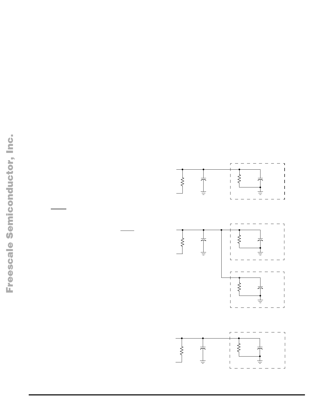
Each secondary transceiver has a 470 ±10% pF capacitor on
its output for EMI suppression purposes, as well as a 10.6 kΩ
±5% pull-down resistor to ground. The primary node has a
3300 ±10% pF capacitor on its output for EMI suppression, as
well as a 1.5 kΩ ±5% pull-down resistor to ground. With more
than 26 nodes, there is no primary node (see Figure 10). All
nodes will have a 470 ±10% pF capacitor and a 10.6 kΩ ±5%
pull-down resistor. No matter how many secondary nodes are
on the Class B bus, the RC time constant of the Class B bus is
maintained at approximately 5.0 µs. The minimum and
maximum capacitance and resistance on the Class B bus is
given by the expressions shown in Table 1, page 10.
One Primary Node
10.6 kΩ 470 pF
1.5 kΩ 3300 pF
Figure 8. Minimum Bus Load
Primary Node
10.6 kΩ 470 pF
1.5 kΩ
3300 pF
24 Secondary Nodes
442 Ω
11280 pF
Figure 9. Maximum Number of Nodes
31 Secondary Nodes
10.6 kΩ 470 pF
342 Ω 14570 pF
Figure 10. Maximum Bus Load
MOTOROLA ANALOG INTEGRATED CIRFCoUIrTMDEoVrICeEIDnAfoTArmation On This Product,
Go to: www.freescale.com
33390
9
Share Link: 