AD720 View Datasheet(PDF) - Analog Devices
Part Name
Description
Manufacturer
AD720 Datasheet PDF : 8 Pages
| |||
AD720/AD721
(continued from page 1)
All required low-pass filters are on chip. After the input signals
pass through a precision RGB to YUV encoding matrix, two on-
chip low-pass filters limit the bandwidth of the U and V color
difference signals to 1.2 MHz prior to quadrature modulation of
the color subcarrier; a third low-pass filter at 3.6 MHz (NTSC)
or 4.4 MHz (PAL) follows the modulators to limit the harmonic
content of the output.
Delays in the U and V chroma filters are matched by an on-chip
sampled data delay line in the Y signal path; to prevent aliasing,
prefilter at 5 MHz is included ahead of the delay line and a post
filter at 5 MHz is added after the delay line to suppress harmon-
ics in the output. These low-pass filters are optimized for mini-
mum pulse overshoot. The overall delay is about 170 ns, which
precompensates for delays in the filters used to decode the
NTSC or PAL signal in a television receiver. (This precompen-
sation delay is already present in TV broadcasts.)
The AD720 and AD721 are available in a 28-pin plastic leaded
chip carrier for the 0°C to +70°C commercial temperature range.
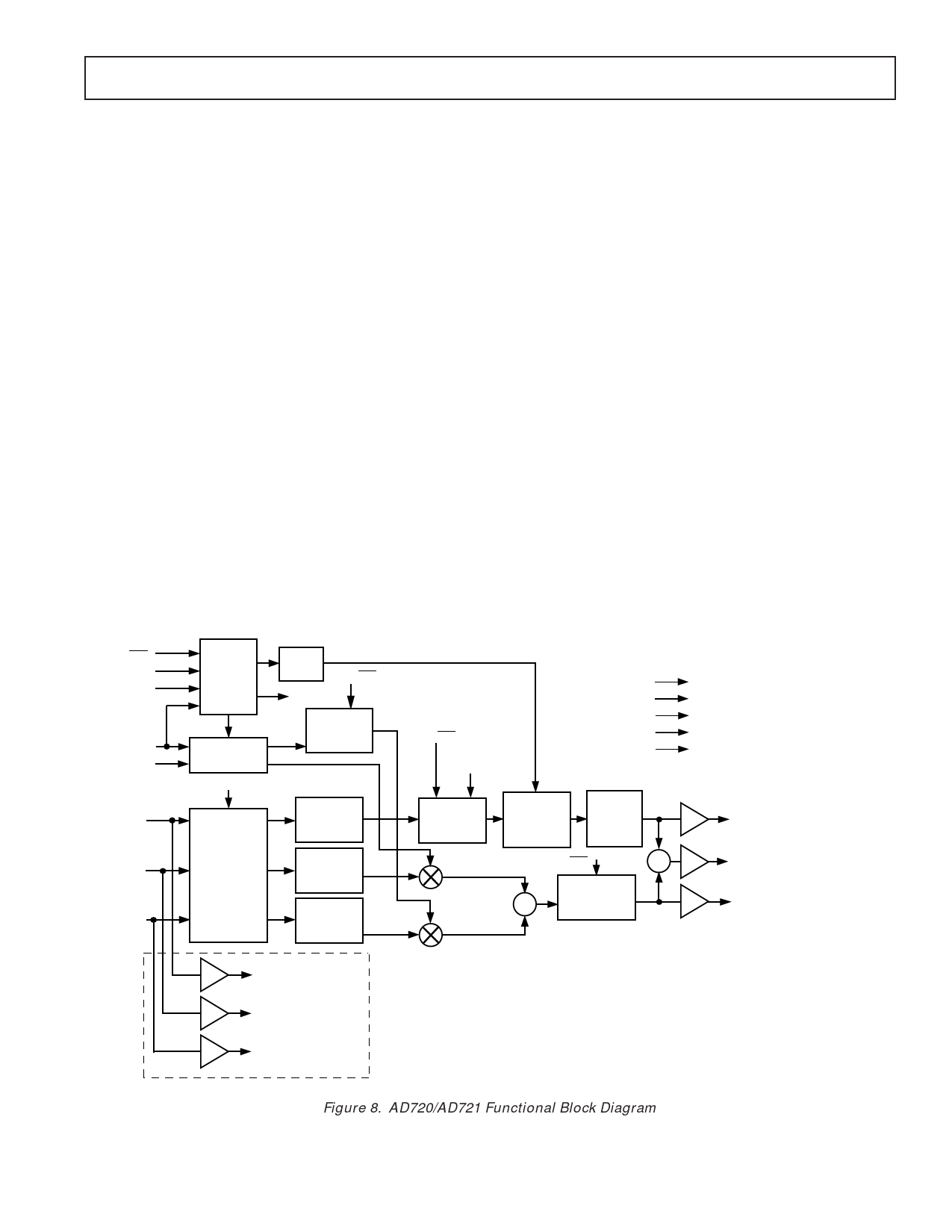
THEORY OF OPERATION
Referring to the AD720/AD721 block diagram (Figure 8), the
RGB inputs (each 0 mV to 714 mV in NTSC or 0 mV to
700 mV in PAL) are first encoded into luminance and color
difference signals. The luminance signal is called the “Y”
signal and the color-difference signals are called U and V. The
RGB inputs are encoded into the YUV format using the
transformation
Y = 0.299R + 0.587G + 0.114B
U = 0.493 (B-Y)
V = 0.877 (R-Y)
For NTSC operation, the chroma amplitude is increased by the
factor 1.06 prior to summation with the luminance output. The
burst signal is inserted into the Y channel in the encoding matrix.
The three outputs of the encoding matrix, now transformed into Y,
U, and V components, take two paths. The Y (luminance) signal is
passed through a delay line consisting of a prefilter, a sampled-data
delay line, and a post filter. The pre- and post-filters prevent
aliasing of harmonics back into the baseband video. The overall de-
lay is a nominal –170 ns relative to the chrominance signal, in
keeping with broadcast requirements to compensate for delays in-
troduced by the filters in the decoding process.
The U and V components pass through 4-pole modified Bessel
low-pass filters with a 1.2 MHz –3 dB frequency to prevent
aliasing in the balanced modulators, where they modulate a
3.579 545 000 MHz (NTSC) or 4.433 618 750 MHz (PAL)
signal via a pair of balanced modulators driven in quadrature by
the color subcarrier.
The AD720/AD721 4FSC input drives a digital divide-by-4 cir-
cuit (two flip-flops) to create the quadrature signal. The refer-
ence phase 0° is used for the U signal. In the NTSC mode, the
V signal is modulated at 90°, but in the PAL mode, the V
modulation input alternates between 90° and 270° at half the
line rate as required by the PAL standard. The outputs of the
balanced modulators are summed and low-pass filtered to re-
move harmonics.
NTSC/PAL
ASNC
C-SYNC
4FSC
ENCD
RED
GREEN
BLUE
SYNC
DECODER
C-SYNC
DELAY NTSC/PAL
BURST
DELAYED C-SYNC
POWER AND GROUNDS
+5V
LOGIC
+5V
ANALOG
QUADRATURE
DECODER
BURST
SC 90°
SC 0°
±180°
(PAL ONLY)
SC 90°/270°
NTSC/PAL
CLOCK
AT 8FSC
–5V
AGND
DGND
ANALOG ONLY
ANALOG
LOGIC
Y
5MHz
4-POLE LP
PRE-FILTER
RGB-TO-YUV U
ENCODING
MATRIX
1.2MHz
4-POLE
LPF
V
1.2MHz
4-POLE
LPF
SAMPLED-
DATA
DELAY LINE
DC
5MHz
RESTORE
AND C-SYNC
2-POLE
LP POST-
X2
INSERTION
FILTER
NTSC/PAL
∑ X2
3.6MHz (NTSC)
∑ BALANCED
MODULATORS
4.4MHz (PAL)
3-POLE LPF
X2
LUMINANCE OUTPUT*
–0.572V TO 1.43V NTSC
–0.6V TO 1.4V PAL
COMPOSITE OUTPUT*
–0.572V TO 2V NTSC
–0.6V TO 2V PAL
CHROMINANCE OUTPUT*
572mVp-p NTSC
600mVp-p PAL
X2
ROUT
1.5Vp-p AD721
(ONLY)
X2
GOUT
1.5Vp-p
X2
BOUT
1.5Vp-p
*NOTE:
THE LUMINANCE, COMPOSITE, AND CHROMINANCE
OUTPUTS ARE AT TWICE NORMAL LEVELS FOR
DRIVING 75Ω REVERSE-TERMINATED LINES.
Figure 8. AD720/AD721 Functional Block Diagram
REV. 0
–5–
Share Link: 