AD720 View Datasheet(PDF) - Analog Devices
Part Name
Description
Manufacturer
AD720 Datasheet PDF : 8 Pages
| |||
AD720/AD721
APPLYING THE AD720/AD721
Figure 9 shows the application of the AD720 and Figure 10
shows the application of the AD721. Note that the AD720 and
AD721 differ from other analog encoders because they are dc
coupled. This means that, for example, the expected RGB
inputs are 0 mV to 714 mV in NTSC and 0 mV to 700 mV in
PAL. The luminance, chrominance, and composite outputs
are also dc coupled. These outputs can drive a 75 Ω reverse-
terminated load. Unused outputs should be terminated with
150 Ω resistors.
The RGB data must be supplied to the AD720/AD721 at
NTSC or PAL rates, interlaced format. Various VGA chip set
vendors support this mode of operation. Most computers supply
RGB outputs in noninterlaced format at higher data rates than
NTSC and PAL, which means that “outboard” encoders must
supply some form of timing conversion before the RGB data
reaches the AD720/AD721.
Note also that the AD720/AD721 does not have internal dc res-
toration and does not accept sync on green. The composite sync
input is a separate, CMOS logical-level input and must be syn-
chronized with the 4FSC input, which serves as the master clock
for the AD720/AD721.
The AD720/AD721 does not implement two elements of the
PAL and NTSC standards. In NTSC operation, it does not
support the 7.5 IRE unit setup (1 IRE unit = 7.14 mV)—this
must be added via software using the RGB inputs. Many RAM-
DACs, such as the Analog Devices ADV471 and ADV478, offer
a logic-selectable setup mode. In PAL operation, the AD720/
AD721 does not implement a 25 Hz subcarrier offset.
Decoupling and Grounding
Referring to the pin descriptions, the AD720/AD721 uses mul-
tiple analog grounds, digital grounds, digital positive supply in-
puts, analog positive supply inputs, and analog negative supply
inputs in order to maximize isolation between analog and digital
signal paths.
The most sensitive input of the AD720/AD721 is the 4FSC pin:
any noise on this pin directly affects the subcarrier and causes
degradation of the picture. Digital and analog grounds should
be kept separate and brought together at a single point.
All power supply pins should be decoupled using 0.1 µF ceramic
capacitors located as close to the AD720/AD721 as possible. In
addition, ferrite beads may be slipped over the power supply
leads to reduce high frequency noise.
If a high speed RAM-DAC is used (e.g., capable of 80 MHz op-
eration with subnanosecond rise times), care must be taken to
properly terminate the input printed-circuit-board traces to the
AD720/AD721. Otherwise, ringing on these traces may occur
and cause degradation of the picture.
APPLICATIONS HINTS
In applying the AD720/AD721, problems may arise due to in-
correct input signals. A few common situations follow.
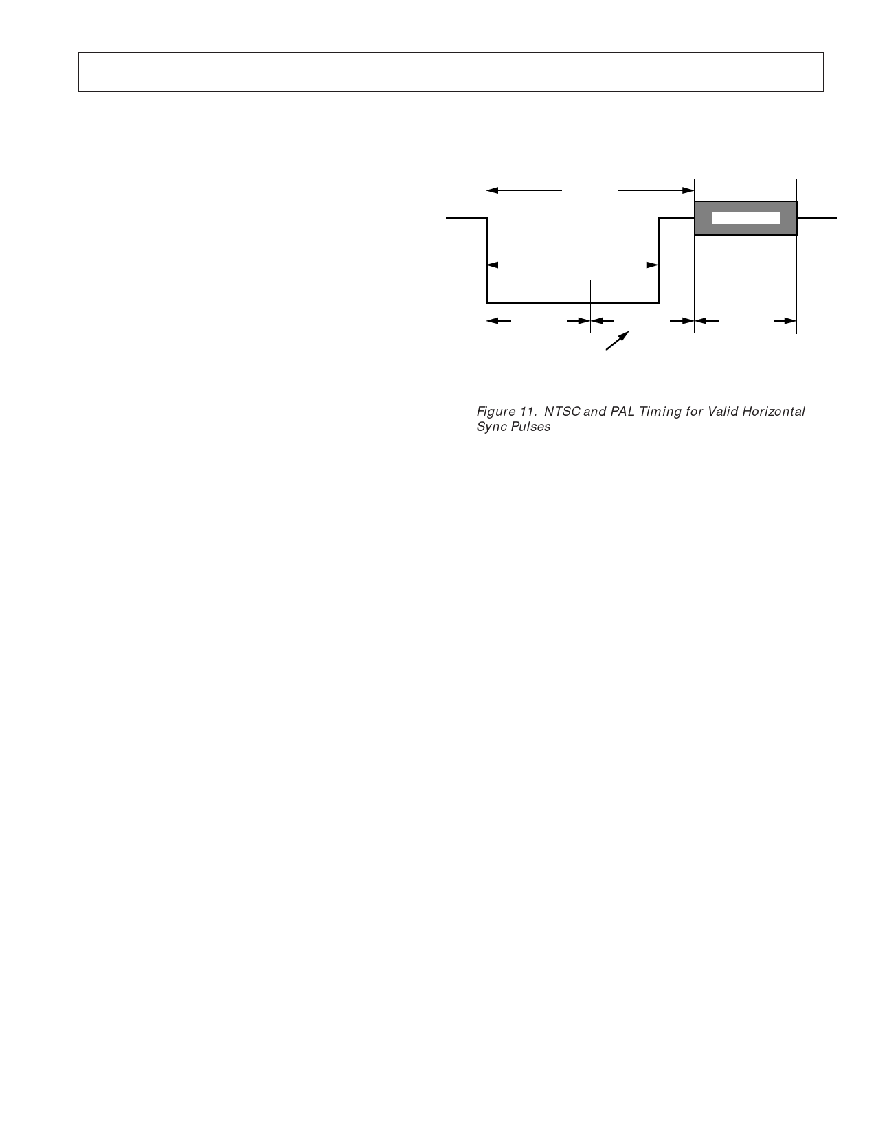
Fade to Black or White—Invalid Horizontal Sync Pulses
Some systems produce sync pulses that are longer or shorter
than the NTSC and PAL standards specify. The digital sync
separator in the AD720/AD721 ignores horizontal sync pulses
that are too long or too short. Figure 11 shows the timing win-
dows for valid NTSC and PAL horizontal sync pulses.
NTSC: 5.30µs
PAL: 5.46µs
COLOR BURST
COMPOSITE SYNC PULSE
NTSC: 2.79µs
PAL: 3.21µs
NTSC: 2.51µs
PAL: 2.25µs
NTSC: 2.51µs
PAL: 2.25µs
IF THE TRAILING EDGE OF A COMPOSITE SYNC PULSE IS WITHIN
THIS WINDOW, THE PULSE IS TREATED AS A HORIZONTAL SYNC PULSE.
IF THE TRAILING EDGE IS OUTSIDE THIS WINDOW, THE PULSE IS TREATED
AS AN EQUALIZING OR BLANKING PULSE.
Figure 11. NTSC and PAL Timing for Valid Horizontal
Sync Pulses
When the horizontal sync pulses are too long or too short, a dc
offset voltage (due to charge storage) increases on the output of
the sampled data delay line’s auto-zero amplifier. Normally, this
offset voltage is removed at the beginning of every line, as signi-
fied by the horizontal sync pulse. Without the horizontal sync
pulse, the dc offset on the auto-zero amplifier increases over
time (usually about three to five minutes) until it overrides the
luminance information. The end result is a slow fade to black or
white.
Color Flickering—Asynchronous Operation
The AD720/AD721 requires that its 4FSC and composite sync
signals be synchronized. In most systems, when the two signals
are synchronized, the composite sync signal is generated using a
4FSC signal as the reference. After every four frames, the
AD720/AD721 resets the phase quadrature generator. When the
CSYNC and 4FSC are synchronized, this reset is transparent to
the system because the reference phase does not change. When
the CSYNC and 4FSC are not synchronized, the difference
between the reference phase and its new value upon reset causes
an instantaneous color shift, which appears as a flickering in the
color.
Adding NTSC Setup
The easiest way to add the 7.5 IRE unit1 setup is to use a
ADV471/478 or ADV477/475 or ADV473 type RAM-DAC,
which have a logic-selectable setup (called “pedestal” on some
data sheets and “setup” on others).
Color Fidelity
A source impedance other than 37.5 Ω (75 Ωʈ75 Ω—a
reverse-terminated 75 Ω input) can cause errors in the YUV
encoding matrix, which is basically resistive and depends on the
correct source impedance for accuracy. Figures 9 and 10 show
the correct interface between a RAM-DAC and the AD720 and
AD721 respectively, using 75 Ω reverse-terminated connections.
NOTE
1IRE unit = 7.14 mV.
REV. 0
–7–
Share Link: 