CYM1831 View Datasheet(PDF) - Cypress Semiconductor
Part Name
Description
Manufacturer
CYM1831 Datasheet PDF : 8 Pages
| |||
CYM1831
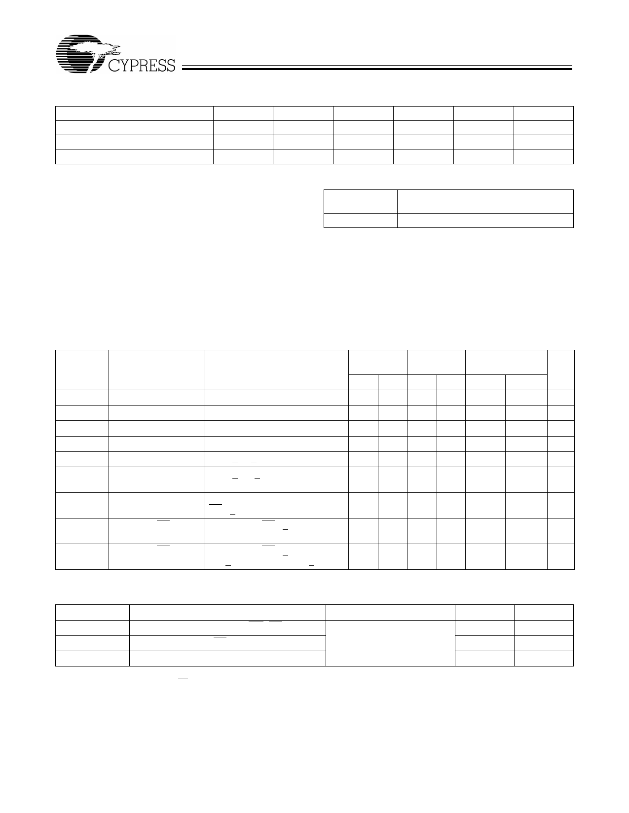
Selection Guide
Maximum Access Time (ns)
Maximum Operating Current (mA)
Maximum Standby Current (mA)
1831-15
15
1120
160
1831-20
20
960
160
1831-25
25
720
160
1831-30
30
720
160
1831-35
35
720
160
Maximum Ratings
(Above which the useful life may be impaired. For user guide-
lines, not tested.)
Storage Temperature ................................. –65°C to +150°C
Ambient Temperature with
Power Applied............................................. –55°C to +125°C
Supply Voltage to Ground Potential ............... –0.5V to +7.0V
DC Voltage Applied to Outputs
in High Z State ............................................... –0.5V to +7.0V
DC Input Voltage............................................ –0.5V to +7.0V
Output Current into Outputs (LOW) .............................20 mA
Operating Range
Range
Commercial
Ambient
Temperature
0°C to +70°C
1831-45
45
720
160
VCC
5V ± 10%
Electrical Characteristics Over the Operating Range
Parameter
Description
Test Conditions
VOH
Output HIGH Voltage VCC = Min., IOH = –4.0 mA
VOL
Output LOW Voltage VCC = Min., IOL = 8.0 mA
VIH
Input HIGH Voltage
VIL
Input LOW Voltage
IIX
Input Load Current GND < VI < VCC
IOZ
Output Leakage
GND < VO < VCC,
Current
Output Disabled
ICC
VCC Operating
VCC = Max., IOUT = 0 mA,
Supply Current
CSN < VIL
ISB1
Automatic CS Pow-
er-Down Current[1]
VCC = Max., CSN > VIH,
Min. Duty Cycle = 100%
ISB2
Automatic CS Pow-
er-Down Current[1]
VCC = Max., CSN > VCC – 0.2V,
VIN > VCC – 0.2V or VIN < 0.2V
1831-15
1831-20
1831-25, 30, 35,
45
Min. Max. Min. Max. Min. Max. Unit
2.4
2.4
2.4
V
0.4
0.4
0.4
V
2.2 VCC 2.2 VCC 2.2
VCC
V
–0.5 0.8 –0.5 0.8 –0.5
0.8
V
–20 +20 –20 +20 –20
+20 µA
–20 +20 –20 +20 –20
+20 µA
1120
960
720 mA
320
320
320 mA
160
160
160 mA
Capacitance[2]
Parameter
Description
Test Conditions
Max.
Unit
CINA
CINB
Input Capacitance (A0–A15, WE, OE)
Input Capacitance (CS)
TA = 25°C, f = 1 MHz,
VCC = 5.0V
80
pF
15
pF
COUT
Output Capacitance
20
pF
Notes:
1. A pull-up resistor to VCC on the CS input is required to keep the device deselected during VCC power-up, otherwise ISB will exceed values given.
2. Tested on a sample basis.
Document #: 38-05270 Rev. **
Page 2 of 8
Share Link: 